Product Description:
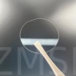
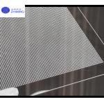
Sapphire Substrate is a high-quality single-crystal substrate
carrier made of Al2O3 material with an ultra-low TTV of less than 5
μm. It is available in both C-plane and M-plane orientation,
providing excellent parallelism of 3 arcsecs. It is the perfect
choice for sapphire windows and sapphire wafer applications. It is
perfect for high-end optical, optoelectronic, and semiconductor
device applications. With its outstanding performance, Sapphire
Substrate is the ideal choice for demanding applications.
Features:
- Product Name: Sapphire Substrate
- Surface Orientation: ±0.5° C-plane and M-plane
- TTV: <5μm
- Material: Al2O3 99.999%
- Warp: <20μm
- Bow: <20μm
- Applications: Sapphire Windows and Sapphire Substrates
Applications:
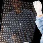
ZMSH's Sapphire Substrate is the perfect choice for your
wafer-level device needs. Our sapphire wafer has a model number of
Sapphire wafer, which is made in China and features a surface
orientation of ±0.5°, a clear aperture of >90%, a surface
roughness of Ra<0.5nm, a surface quality of single side
polished, and a perpendicularity of 3 arc sec. With its superior
quality and reliable performance, it is the perfect substrate for
your wafer-level device needs.
Technical Parameters:
| Parameters | Description |
|---|
| Name | Sapphire Wafer Substrate Carrier |
| Material | Al2O3 99.999% |
| Substrate Type | Single Crystal |
| Size | 1inch 2inch 3inch 4inch 6 Inch 8inch 12inch |
| Thickness | 0.1-5mm |
| Bow | <20μm |
| TTV | <5μm |
| Flatness | λ/10@633nm |
| Parallelism | 3 Arc Sec |
| Clear Aperture | >90% |
| Keywords | Sapphire wafer, sapphire windows, C-plane M-plane, wafer
fabrication, crystal growth, opto-electronic, substrate carrier,
single crystal |
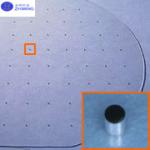
2inch C-plane (0001)SSP 0.43mm Single side polished Sapphire
substrates
| No | Properties | Target | Tolerance |
|
| 1 | Diameter | 50.8mm | ± 0.1mm |
| 2 | Thickness | 430μm | ±15μm |
| 3 | Surface orientation of C-plane | off C-axis to M0.2° | ± 0.1° |
| 4 | Primary flat length | 16mm | ±11mm |
| 5 | Primary flat orientation | A-plane(11-20) | ±0.1° |
| 6 | Back side Roughness | 0.8~1.2um | |
| 7 | Front side Roughness | <0.3nm |
| 8 | Wafer edge | R-type |
| 9 | Total Thickness Variation, TTV | ≤ 10μm(LTV≤5μm,5*5) |
| 10 | SORI | ≤10μm |
| 11 | Bow | -10 μm ≤ BOW ≤ 0 |
| 12 | Laser Mark | N/A |
| | | Package | 25 wafers in one cassette |
|
| Trace ability | Wafers shall be traceable with respect to cassette number |
|
We specialize in providing customized services for ZMSH Sapphire
Substrate with high Clear Aperture and Surface Roughness of
<0.5nm, and Bow and Warp of <20μm, available in C-plane.
A-plane, M-plane, R-plane 2inch,3inch, 4inch 6inch, 8inch 12inch.
Packing and Shipping:
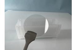
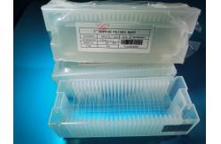
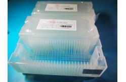
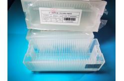
Sapphire Substrate Packaging and Shipping
Sapphire substrates are shipped in clean and safe plastic
containers. The containers are marked with the product name,
product quantity, and product dimensions. The container is then
sealed with a plastic cover to keep the product free from dust and
dirt.
The containers are carefully packed in corrugated cardboard boxes
for safe shipping. The box is marked with the customer's address,
the product name, and the number of containers. The dimensions of
the box are also marked on the box.
The shipping company is responsible for delivering the product to
its destination. The customer is responsible for any additional
fees associated with the shipping.