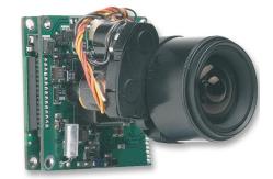
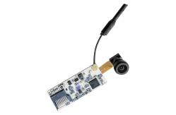
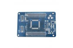
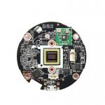
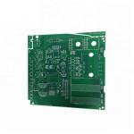
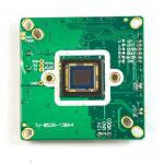
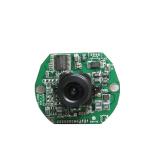
Multilayer Circuit Board cctv camera mould pcb pcba made of gerber
file bom PCBA Manufacturing Service
PCB files, PCB technical requirements, BOM, Assembly or soldering
technical requirements, to be offered by customer.
One Stop PCBA service: Production of PCB from 1-32 Layer, Assembly
components/material purchase, SMT production, PCBA Testing, PCBA
aging,PCBA Packaging, PCBA Delivery.
PCBA Manufacturing Delivery Duration
Delivery for samples will be 10-15 WD after OEM Contact is signed
and the Engineering Documents are confirmed.
For Mass production, based on the customer requirements, delivery
can be done in several steps (Partial Delivery).
PCBA Manufacturing Additional Information
1. After the confirmation of Prototype, MP will be started.
2. DIP Components will be positioned only once, minimum distance
between components and PCB Board will be maintained.
3. Positioning Holes and Grounding holes will be protected by high
temperature resistance tape.
4. EPE Antistatic packaging is used to prevent shock and other
problems.
About us Shenzhen Jingchuang Electronics Co., Ltd., a professional PCB
proofing manufacturer and small and medium-sized batch manufacturer
from Shenzhen, China, was established in 2010. It is a one-stop
service dedicated to reverse engineering, PCB rapid proofing,
component procurement and PCB assembly. high-tech enterprises,You
will be expected to save 5% to 25% of the cost. PCB Process capability
| | Item | Capability | Details | | Number of layers | 1-6 copper layers PCB prototypes | The number of layers refers to the number of layers in the design
document, which can produce 1-6 layers of through-hole plate | | Material | Cardboard, semi-glass, full glass (FR-4), aluminum substrate | | | Max. Dimension | 650x520mm/640x480mm | The maximum size of single and double sided is 650x520mm, and the
maximum size of four or six layers is 640x480mm. | Dimension Tolerance
(Outline) | ±0.15mm | CNC:±0.15mm , V-cut :±0.15mm | | Thickness | 0.4--2.0mm | 0.4/0.6/0.8/1.0/1.2/1.6/2.0 mm | Thickness Tolerance
( Thickness≥1.0mm) | ± 10% | e.g. For the 1.6mm board thickness, the finished board thickness
ranges from 1.44mm(T-1.6×10%) to 1.76mm(T+1.6×10%) | Thickness Tolerance
( Thickness<1.0mm) | ±0.1mm | e.g. For the 0.8mm board thickness, the finished board thickness
ranges from 0.7mm(T-0.1) to 0.9mm(T+0.1). | | Minimum line width | 4mil(0.1mm) | Currently available for 4mil line width, line width is recommended
to be greater than 4mil | | Minimum clearance | 4mil(0.1mm) | At present, 4mil line spacing can be connected, and the gap is
recommended to be larger than 4mil
| | Finished Outer Layer Copper | 35um/70um(1 OZ/2 OZ) | Finished outer layer copper weight is 1 OZ=35um,2 OZ=70um | | Finished Inner Layer Copper | 0.5 oz (17um) | Finished inner layer copper weight is 0.5 oz only | | Min. Via hole size | 0.25mm | For Single&Double Layer PCB, the minimum via hole size is
0.3mm;
For Multi Layer PCB, the minimum via hole size is 0.2mm. | | Min. Via diameter | 0.45mm | For Single&Double Layer PCB, the minimum Via diameter is 0.6mm;
For Multi Layer PCB, the minimum via diameter is 0.45mm. | | Via To Trace | ≥5mil | Minimum distance between via(plated holes) and trace is 5mil. | | Drill Hole Size | 0.2--6.3mm | Min. drill size is 0.2mm, Max. drill size is 6.3mm. | | Hole Size Tolerance | ±0.08mm | e.g. For the 0.6mm hole, the finished hole size between 0.52mm to
0.68mm is acceptable. | | Annular Ring | ≥3mil | Annular ring surrounded by traces should be equal to or larger than
3mil | | Min. Character Width | ≥6mil | Characters width less than 6mil(0.153mm) will be unidentifiable | | Min. Character Height | ≥32mil | Characters height less than 32mil will be unidentifiable. | | Trace to Outline | ≥0.2mm | Ship as individual board(Routing): Trace to Outline ≥0.2mm; Ship as
panel with V-scoring: Trace to V-cut line ≥0.4mm | | Panelization without space | 0mm | | | Panelization with space | ≥2mm | Make sure the space between boards should be ≥2mm, otherwise it
will be hard to process for routing. | | Min. Edge Rails | 3mm | | | Min. Half Hole Diameter | 0.6mm | Half hole is a special technology, so half hole diameter should be
greater than 0.6mm. |
| SMT processing capability | | Item | PCBA processing capacity
| | Lead Time | | elivery time is 24 hours (fastest 6 hours expedited), small batch
delivery is 5 days, all the above time after all components and PCB
materials are ready Start the calculation immediately. | | Production capacity | SMT patch 4 million points / day, plug-in after welding 500,000
points / day, 50-100 styles / day | | Parts Source | Consigned/kitted | We hope that you will supply all the parts for the PCBA service. In
this case, please send us all the components with the BOM file and
a detailed packing list, which should include the item number in
the kit, the part number and quantity of the customer or
manufacturer. With a mature and effective component procurement
management system. A team of professional procurement engineers and
experienced purchasing staff is responsible for the procurement and
management of parts for our customers. Customers choose our
complete set of alternative materials, which greatly reduces
procurement costs and management costs, eliminating the hassle of
multi-party communication and improving work efficiency. | | Turn-key | With our wide and powerful network of parts sourcing, we offer
Turn-key PCBA service. We do not mark up on the parts cost.
Considering the big price gap between different suppliers, we only
source from reliable suppliers who may have no price advantages. We
will always ask for your approval before making any decisions. | | Partial Turn-key/Combo | This is our regular practice which you offer the main devices and
components, while we source the rest for you. Just like the
Turn-key service, we will ask for your approval on every details of
the parts concerning price, quality and availability. | | Assembly Options | We offer Surface Mount (SMT), Thru-Hole (THT) and hybrid of both.
We also offer single or double-sided placement. | | Types of Solder | We offer both leaded and lead-free (RoHS Compliant) assembly
services for our customers. Please choose one to best fit your PCB
and the parts on the PCB. | | Stencils | We use laser cut stainless steel stencils to ensure high
reliability for fine pitch and BGA components. Nano coating is
available upon request. | | Minimum Order | Our minimum is as low as 5 pieces. We do not want you to pay for
what you do not need indeed to save you money. | | Component Size | Passive Component: we can accept components as small as 01005,
0201,0402.
BGA: We have the ability to handle BGA of 0.25mm pitch with X-ray
testing.
Fine Pitch Parts: we can assemble 0.25mm fine pitch parts. | | Component Package | We accept parts in Reels, Cut Tape, Tube & Tray, Loose Parts
and Bulk. | | Maximum part placement accuracy(100FP) | Full placement accuracy of ±50 microns, repeatability up to ±30
microns | PCB board type
| PCB hard Board(FR-4,Metal substrate),PCB Soft board(FPC),soft and
hard board PCB | | Board Dimension | Min Board Size: 50mm x 100mm (Boards smaller than this size need to
be panelized)
Max Board Size: 250mm x 500mm | | file format | List of materials/components (BOM),PCB(Gerber Files and most PCB
design format files), coordinate files) | Test
| Before delivery, we will apply a variety of test methods to PCBA in
or already mounted: | | • IQC:Material inspection | | • IPQC:Production sampling check | | • QC:Routine quality inspection | | • AOI:Check solder paste, solder effect of patch elements, missing
parts or components polarity | | • X-Ray:Check high-precision hidden PAD components such as BGA and
QFN; | • Functional testing: test functions and performance according to
customer test procedures and procedures to ensure compliance.
| •aging testing: test functions and performance according to
customer test procedures and procedures to ensure compliance.
| | Repair & Rework | Our BGA repair service can safely remove defective BGA, such as
dislocation, offset, virtual welding, and so on, and put it
perfectly on the PCB again.
|
|