
Mechanical Grade Technical Ceramic Parts InP Wafer Indium Phosphide
|
|
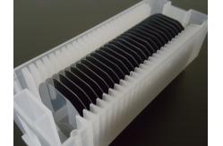
InP wafer ( Indium phosphide )
We provides high quality single crystal InP wafer ( Indium phosphide ) to micro-electronic ( HBT/ HEMT ) and opto-electronic industry ( LED / DWDM / PIN / VCSELs ) in diameter up to 3 inch . Indium phosphide ( InP ) crystal is formed by two elements , Indium and Phosphide , growth by Liquid Encapsulated Czochralski ( LEC ) method or VGF method . InP wafer is an important semiconductor material which have superior electrical and thermal properties , compared to silicon wafer and GaAs wafer , InP wafer has higher electron mobility ,higher frequency , low power consumption , higher thermal conductivity and low noise performance . We can provide epi ready grade InP wafer for your MOCVD & MBE epitaxial application .Please contact us for more product information .
III-V Compound Wafer We provides a wide range of compound wafer including GaAs wafer, GaP wafer, GaSb wafer, InAs wafer, and InP wafer .
Electrical and Doping Specification Product Specification
|
||||||||||||||||||||||
| Product Tags: Technical Ceramic Parts InP Wafer Mechanical Grade InP Wafer InP Wafer Indium Phosphide |

|
Carbon Fiber Insulation Graphite Felt for Industrial Applications |

|
C-C Composite Material for High-Temperature Industrial Applications |

|
High Purity Graphite for Semiconductors and Solar Energy |
|
Aluminum Nitride Structural Ceramic Parts High Strength |
|
Aluminum Nitride Ceramic Substrate High Thermal Conductivity |
|
High Pressure Pump Valve Assembly for Hydraulic Systems |