
4 Layers Single Double Side PCBA Printed Circuit Board Assembly
|


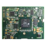
FR-4 Multilayer Pcb 4 Layers Pcba Single And Double Side PCB Assembly
Double Side PCB Assembly IntroductionThe double-sided printed circuit board (also double-layer board)provides on both side conductive paths for assembly of components, then to fabricate the PCB'A. Our engineers is qualified and experienced in producing surface-mount (SMT), through-hole (THT) and mixed-technology components and fine-pitch parts and ball grid arrays (BGAs) for high-density FR-4 PCBs .
PCB CAPABILITIES
PCBA CAPABILITIES
Our SMT capabilities:
SMT Assembly: SMT provides a flexible high technology. These solutions include: 7 high-speed placement machines, 7 automatic printers with fiducial alignment, 2 X-ray machines, BGA maintenance machines, ICT test machines
Our DIP function:
A-8 semi-assembly production line with four wave soldering machines 1 U-shaped automatic assembly line for box-type building products with test stations High temperature / low temperature aging test furnace B-4 for products required for aging test With time control and temperature control All products are 100% inspected and tested during the DIP process Haina lean Electronics Co.,Ltd is a competitive China customize pcba for medical breathing machine OEM manufacturer, supplier and vendor, you can get quick turn customize pcba for medical breathing machine production prototypes and samples from our factory. Hot Tags: customize pcba for medical breathing machine, China, supplier, manufacturer, factory, OEM manufacturer, vendor, samples, production, prototypes, quick turn
Double Side PCB Assembly Process
1.Solder Paste stenciling---2.Surface Mount Technology (Pick and Place)---3.Reflow Soldering---4.Inspection and Quality Control---5.Through-Hole Component Insertion (DIP Process)---6.Final Inspection and Functional Test
Our advantage
1.Service value Independent quotation system to quickly serve the market 2.PCB manufacturing High-tech PCB and PCB assembly production line 3.Material purchasing A team of experienced electronic component procurement engineers 4.SMT post soldering Dust-free workshop, high-end SMT patch processing
Electronic Board Assembly Delivery Time
PCB Assembly Application Field
Our products are widely used in the following areas: 1. communication equipment, 2. industrial control, 3.consumer electronics, 4.medical equipment, 5. aerospace, 6.light-emitting diode lighting, 7.automotive electronics etc
Workshop
Partners
Common packaging
1.PCB: Vacuum packaging with carton box
|
||||||||||||||||||||||||||||||||||||||||||||||||||||||||||||||||||||||||||||||||||||||||||||||||||||||||||||||||||||||||||||||||||||||||||||||||||||||
| Product Tags: 1mm PCBA Printed Circuit Board Assembly ROHS PCBA Printed Circuit Board Assembly 4 Layers PCBA Module | ||||||||||||||||||||||||||||||||||||||||||||||||||||||||||||||||||||||||||||||||||||||||||||||||||||||||||||||||||||||||||||||||||||||||||||||||||||||
|
FR4 ENIG BGA EMS Double Side Electronics PCB Assembly |

|
Double Side FR4 HASL Electronic Rigid PCB Assembly |

|
0.5OZ FR4 HDI Double Side PCB Assembly |

|
FR4 HASL Pb Free Double Sided SMT Assembly |

|
2 Layer 1.6mm Double Sided PCB Assembly |

|
HF FR4 OSP 4 Layer Double Side PCB Assembly , 2oz Quick Turn PCB Assembly |