
4 Layer PCBA SMD SMT DIP Through Hole PCB Assembly
|


4 layer PCBA Multilayer SMD SMT DIP Through-Hole Process PCB AssemblyThrough-Hole Process PCB Assembly Introduction
Through-hole PCB assembly are the key in many mission-critical
electrical assemblies.
Our engineers is qualified and experienced in producing surface-mount (SMT), through-hole (THT) and mixed-technology components and fine-pitch parts and ball grid arrays (BGAs) for high-density FR-4 PCBs . Max layer count: 46L
PCB CAPABILITIES
PCBA CAPABILITIES
Our SMT capabilities:
SMT Assembly: SMT provides a flexible high technology. These solutions include: 7 high-speed placement machines, 7 automatic printers with fiducial alignment, 2 X-ray machines, BGA maintenance machines, ICT test machines
Our DIP function:
A-8 semi-assembly production line with four wave soldering machines 1 U-shaped automatic assembly line for box-type building products with test stations High temperature / low temperature aging test furnace B-4 for products required for aging test With time control and temperature control All products are 100% inspected and tested during the DIP process
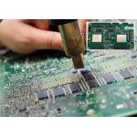
PCB Assembly Process
1.Solder Paste stenciling
Why choose us?
Reliable PCB Manufacturing & Assembly; Quality PCB Fabrication; Best On Time PCB Shipping Record; Financially Stable PCB Company; 24 Hour Tech Support; PCB Instant Quoting; Easy PCB Order Status Tracking; No Minimum PCB Order Requirements; Waived Tooling Charges; Free PCB Design Software & Free File Check.
Our advantage
Service value: Independent quotation system to quickly serve the market PCB manufacturing: High-tech PCB and PCB assembly production line Material purchasing: A team of experienced electronic component procurement engineers SMT post soldering: Dust-free workshop, high-end SMT patch processing
Delivery Time
Through-Hole Process PCB Assembly Application Field
PCB Assembly are widely used in communication equipment, industrial control, consumer electronics, medical equipment, aerospace, light-emitting diode lighting, automotive electronics.
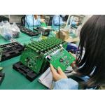
Workshop
Partners
Common packaging
FAQ
FAQ 1.What are needed for quotation? 2. What file formats do you accept for production? 3.Are my files safe? 4.MOQ? 5.Shipping Cost ? The shipping cost is determined by the destination ,weight ,packing size of the goods .We can provide shipping, air, land, express and other transportation services . 6.How to ensure high-quality production? Q7.What are the services you can provide ? One-stop contract manufacturing Yes , we will test each piece of PCBA product under your testing methods ,to ensure quality and functionality . Q9.Do you provide OEM service ? Yes ,we offer PCB and PCBA OEM Service , we manufacture the PCB and PCBA products to your design and requirements .
Company Information
Haina lean Electronics Co., Ltd is a one-stop EMS supplier integrating PCB design, PCB manufacturing, Component sourcing and PCB assembly. Our company was established in May 1, 2006 in Beijing. And expansion was completed in June 2016. The company is specialized in electronic products supporting processing services, mainly to undertake circuit board design, layout production, components procurement, PCB plate making, circuit board welding assembly debugging and other OEM/ODM services.
Our first factory is located in Changping District, Beijing, the main radiation Haidian, Changping, Chaoyang three areas of Beijing. Since our company’s establishment, we have been adhering to creating high quality, high efficiency, low-cost business philosophy based on the circuit board processing industry for customers. Most of the key staff of the company are mature technical talents who have been engaged in the industry for more than 10 years, and have rich experience in the production of SMT and DIP, also has rich experience in production for high density & difficulty to package components such as BGA. We obtain a good reputation in the industry through the continuous efforts from all staff and high quality service . Our second branch plant is located in Langfang city, and mainly cover Fengtai and Daxing Yizhuang area. Our factory covers an area of 6000 square meters.
Our company pursues "inclusiveness, excellence, people-oriented". Constantly innovate, take technology as the core, regard quality as life, and wholeheartedly provide customers with high-quality and high-efficiency humanized services.We are willing to serve our customers with the principle of continuous honesty & trustworthiness, pragmatism and innovation.
|
||||||||||||||||||||||||||||||||||||||||||||||||||||||||||||||||||||||||||||||||||||||||||||||||||||||||||||||||||||||||||||||||||||||||||||||||||||||
| Product Tags: ISO16949 Through Hole PCB Assembly 4 Layer Through Hole PCB Assembly THT PCB Printing And Assembly | ||||||||||||||||||||||||||||||||||||||||||||||||||||||||||||||||||||||||||||||||||||||||||||||||||||||||||||||||||||||||||||||||||||||||||||||||||||||

|
Oem 1oz Multilayer Smt Through Hole Pcb Assembly Soldering |

|
Ems Smt Fr4 Circuit Board Through Hole Pcba Components |
|
4 Layer Odm Fr4 Tht Prototype Through Hole Pcb Assembly |

|
Enig Prototype Through Hole Pcb Assembly For Industrial Control Equipment |
|
Fr4 4Layer Pcb Assembly Multilayer Circuit Board through hole |

|
Cem-1 Gold Finger 700x610mm Fr 4 Pcb Assembly With X-Ray Inspection |