
Fast Integration Thermal Imaging Camera Module 384x288 17μM For Health Care
|
|
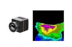
iHA417W Medical Diagnosis Thermal Module
Product Description
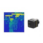
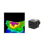
iHA417W thermal module is specially developed for medical diagnosis. It is integrated with self-developed wafer level packaging 384×288/17μm infrared detector, 9.1mm lens, 30pin standard interface (Optional Type-C expansion board) and a dedicated SDK for medical temperature measurement.
There are two modes of temperature measurement distance: 5 meters and 0.5 meters, which can be used in various scenarios. The iHA417 medical diagnosis thermal module has a better temperature measurement consistency and superior temperature measurement accuracy of ±0.5°C. No need for built-in black body ensures a compact design and easier temperature measurement.
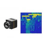
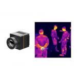
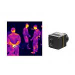
The iHA417W thermal camera module can be quickly integrated into various medical thermal imaging devices, and it is expected to be widely used in the fields of Disease Screening, Traditional Chinese Medicine Physiotherapy, Health Check-up, Rehabilitation etc. at present and in the future.
Main Features
Product Specifications
Detect Distance Industrial Applications Our Advantages
FAQs
1. About metal packaging infrared detector Metal packaging uses metal tube shell, thermoelectric cooler (TEC) and columnar getter. The TEC plays an important role of stabilizing the working temperature so that the infrared detector works at room temperature, thereby improving the ability of thermal imaging sensors to adapt to extreme environments, such as heavy fog, rain and snow etc.
But the disadvantage is that the cost is too high, accounting for more than 60% of the total cost of the entire uncooled products production, and causing a long production cycle. Such packaging method is for high-end applications.
2. About ceramic packaging infrared detector Ceramic packaging process is similar to metal packaging, which is a mature infrared detector packaging technology. Compared with metal packaging, the volume and weight of the packaged detector will be greatly reduced. For ceramic packaging, its readout circuit has self-adjusting operating temperature function and does not require TEC stabilization.
3. Wafer Level Packaging Wafer-level packaging, also known as wafer-level size packaging, has become an important part of advanced packaging technology in the semiconductor industry. Wafer level packaging (WLP) is the process of completing high vacuum packaging directly on the entire MEMS wafer, then scribing and cutting to make a single infrared detector. It performs most or all of the packaging and testing procedures directly on the IR detector wafer before dicing. It is an improved chip size package that meets the needs of small size, lightweight, portable, handheld, low price and high production efficiency. |
||||||||||||||||||||||||||||||||||||||||||||||||||||||||||||||||||||||||
| Product Tags: 17uM Thermal Imaging Camera Module Thermal Imaging Camera Module 384x288 Fast Integration Thermal Camera Module | ||||||||||||||||||||||||||||||||||||||||||||||||||||||||||||||||||||||||

|
Fast Integration Thermal Imaging Camera Module 384x288 17μM For Health Care |
|
Body Temperature Screening Uncooled Thermal Camera Module 384x288 17μM |
|
384x288 17μM Uncooled Thermal Module For Medical Thermal Image Screening |
|
Fast Integration Thermal Module For Large Scale Body Temperature Screening |
|
384x288 17μM Thermal Imaging Camera For Non Invasive Early Disease Diagnosis |
|
Radiation Free Infrared Camera Module For Medical Thermal Image Screening |