
Tg150 Fr4 Soldering Double Sided Pcb 4oz Heavy Copper 2.4mm Thickness
|


Electronic Board, Rogers PCB, Rogers, High Performance, RF Identification Tags,Multi-LayerAbis Circuits Co. Ltd is a great PCB manufacturer that was established in 2006 and is based in Shenzhen (China’s “Silicon Valley”).
What is the feature of Heavy Copper PCB? The vast majority of thick copper plates are high-current substrates (current x voltage = power). The main application areas of high-current substrates are two major areas: power modules (power modules) and automotive electronic components. Some of its main terminal electronic products are the same as conventional PCBs (such as portable electronic products, network products, base station equipment, etc.), and some are different from conventional PCB fields, such as automobiles, industrial control, and power modules, etc.
High-current substrates differ from conventional PCBs in efficacy. The main function of a conventional PCB is to form wires that transmit information. The high-current substrate has a large current passing through it, and the main function of the substrate carrying the power device is to protect the current-carrying capacity and stabilize the power supply. The development trend of such high-current substrates is to carry larger currents, and the heat emitted by larger devices needs to be dissipated, so the large currents passing through are getting larger and larger, and all the copper foils on the substrates are getting thicker and thicker. The 6oz copper thickness of the high-current substrates manufactured now has become routine.
What certificate does ABIS have?
We have ISO14001, ISO9001, UL, cUL, and TS16949. You can see more in our company profile.
What are the application fields of Heavy printed Circuit boards? The application fields of thick copper circuit boards are mobile phones, microwaves, aerospace, satellite communications, network base stations, hybrid integrated circuits, power high-power circuits, and other high-tech fields.
What capacity does ABIS have?
What is your Lead Time?
We are not only good at product quality but also FINANCIALLY FIT
because we pay attention to goodwill since 2006 in this opening
city-Shenzhen, China.
|
|||||||||||||||||||||||||||||||||||||||||||||||||||||||||||||||||||||||||||||||||||||||||||||||||||||||||||||||||||||||||||||||||||||||||||||||||||||||||||||||||
| Product Tags: heavy copper soldering double sided pcb 2.4mm thickness soldering double sided pcb tg150 double sided fr4 pcb | |||||||||||||||||||||||||||||||||||||||||||||||||||||||||||||||||||||||||||||||||||||||||||||||||||||||||||||||||||||||||||||||||||||||||||||||||||||||||||||||||

|
ROHS FR4 Double Side PCB Multilayer Printed Circuit Board Impendance Control |

|
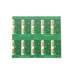
Gold Finger PRINTED Double Sided PCB Quick Turnaround |
|
Gold Finger Circuit Board PCB Board Quick Turnaround 30U'' |

|
Matt Black 2 Layer Circuit Board PCB Assembly FR4 TG150 |

|
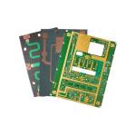
RoHS Custom Single / Double / Multilayer 94V0 PCB Circuit Board |
|
175um Aluminum Double Sided PCB FR4 CEM1 Alu High CTI250 CTI600 LPI PTEF |