
Heavy Copper Printed Circuit Boards PCB Manufacturing Companies
|
Heavy Copper Printed Circuit Boards PCB Manufacturing Companies
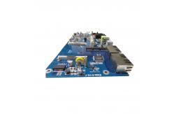
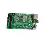
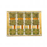
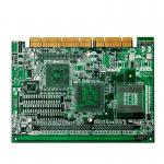
Heavy Copper Printed Circuit Boards PCB Manufacturing FASTPCBA has been building heavy copper circuit boards with traces and copper planes of up to 6 ounces for more than 20 years. Our expertise is in producing at a reasonable cost heavy copper PCBs. Our engineering team can work with you to review your design to make sure that they can be manufactured with the highest quality at the best overall cost.
All options are available at FASTPCBA
Production Minimums
Heavy Copper Circuit Boards Application
* Welding Equipment
Contacting FASTPCBA for Your Heavier Copper Circuit Boards |
||||||||||||||||||||||||||||||||||||||||||||||||||||||||||||||||||||||||||||||||||||||||||||
| Product Tags: PCB Bare Board Manufacturing Prototype PCB Manufacturing Service Heavy Copper PCB Manufacturers |
|
HAL 152.4mil Electronic Circuit Pcb Board FR4 Pcb Prototype Board |

|
OEM FR4 4oz Electronic Printed Circuit Board Rigid PCB |

|
SMD Single Sided 1 Layer Prototype PCB Manufacturing And Assembly |
|
Custom Circuit Board Maker Pwb Printed Wiring Board Pwa Printed Wiring Assembly |
|
Main Board ENIG HASL Lead Free PCB Manufacturing Circuit Board Company |
|
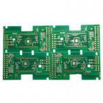
Turnkey High TG PCB Board Fr4 Printed Circuit Board Manufacturer |