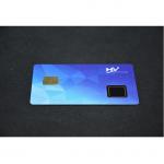
Contact Chip Card: Contact Chip Card With Customizable Shape,
Encryption And Tamper Proof
Contact Chip Card Introduction:
The multi-function application of contact chip card is also an
important advantage of it. The chip adopts a computer frame
structure and can realize different functions. For the
security of smart cards, the EMV standard has formulated a series
of security measures such as bank-to-card authentication,
card-to-host system authentication, and terminal-to-card
authentication, and the length of the key is continuously
increased, making the copying difficulty and cost of smart cards
much higher than that of magnetic stripe cards. Secondly, the
security standards provided by EMV and the processing power and
storage capacity of smart cards provide the possibility for offline
payment. It not only saves transaction costs and transaction time,
but also effectively reduces the dependence of card transactions on
communication networks, realizes dual offline payment, and reduces
the pressure on bank transaction systems.
Contact Chip Card Parameters | Contact Chip Card Type | Active / passive |
| Screen | Electronic Paper / Glass / OLED screen |
| Screen size | 1.02 inch / 1.54 inch / 2.7 inch Section screen / dot screen |
| Appearance color | Customizable layout |
| Thumbprint module | IDEX/FPC |
| Beacon tips | Led prompt light [red, blue] |
| Interface | 7816 interface (optional) |
| RFID | 13.56mhz |
| NFC | Optional |
| Working frequency | 13.56mHz |
| Operating temperature | -20~70 ℃ |
| Encapsulation material | PVC ABS PETG (Select) |
| Bluetooth | Optional |
| Waterproof grade | IP68 industrial waterproof |
| Number of keys | 5 bits / 13 bits |
| Ultra thin lithium battery | >80mah (as required) |
| Charging mode | Magnetic suction / wireless charging / solar charging |
Contact Chip Card PCBA Sealing Process:
Packaging PCBA into smart card has been a technical difficulty in
the smart card industry for many years. The high-temperature
melting PVC method used in the traditional smart card manufacturing
process can no longer meet the PCBA circuit board business card
printing. The high temperature of the traditional process will lead
to problems such as lithium battery failure and component damage.
Heyang technology began to establish a special scientific research
team in 2014, Tackling the PCBA card sealing technology, through
continuous research, we have developed the relevant technologies
and equipment for PCBA card sealing and the corresponding glue
formula. Using the PCBA card sealing technology achievements of
Heyang for many years, we have successfully encapsulated the
ultra-thin lithium battery, chip, solar panel, fingerprint, ink
screen and other components or modules with high performance, high
reliability and flat appearance at room temperature The daily
production capacity of high-end smart cards that meet the bending
test standards has reached 20000-30000 PCS. with the continuous
efforts of Heyang, the production capacity, process and performance
have been gradually improved and improved.
Contact Chip Card FAQ:
1. Q: Are you a factory or trading company?
A:We are a factory.
2. Q: Where is your factory located? How can I visit there?
A: Our factory is located in shenzhen, guangdong Province, China.
All our clients, from home or abroad, are warmly welcome to visit
us!
3. Q: Can we costomize the size, color, logo and package of the
product?
A: Yes, all of these can be cusomized according to your needs.
4. Q: How about your quality control?
A: Our company has obtained CB ROHS certification.
5. Q: What is your MOQ?
A: Any quantity is acceptable for your order. And the price is
negotiable for large quantity.
6. Q: What about the lead time?
A: 3-5 days for sample preparation and 10-15 working days for mass
production.
7.Q: What is your product apply fields?
A: Our products are suitable for schools, nursing homes, hospitals,
finance, buses, hotels and other occasions.