
Fast Turnkey IoT PCB LEAD FREE HASL Hot Air Solder Leveling
|
|
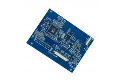
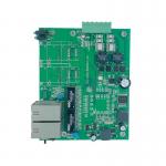
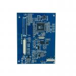
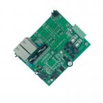
Fast Turnkey IoT PCB LEAD FREE HASL Hot Air Solder Leveling CKS has always been focusing on the design and production of high-end circuit boards, providing customers with professional and efficient one-stop turnkey solutions.Shenzhen Changkeshun Technology Co, Ltd. is a high-tech enterprise engaged in electronic OEM/ODM PCBA process. Shenzhen Changkeshun Technology Co, Ltd. is a hightech enterprise engaged in the processing of electronic OEM/ODM pcba assembly, with over 10 years experience, mainly focused on one stop service including pcb fabrication,electronic components sourcing, pcba assembly function test and end product assembly. We undertake various fields of electronic pcb/pcba manufacturing from smart home system, consumer electronics, vehicle electronics,communication,industrial control, medical, security.We commit to strict control system under ISO9001 and Rohs.
Specification
All test before shipping
Exhibition photos
Product usage
Packaging&Shipping CKS is not only trying to give customers a good product, but also pay attention to offering a complete and safe package. And here we prepare some personalized services for all the orders.
|
|||||||||||||||||||||||||||||||||||||||||||||||||||||||||||||||||||||||||||
| Product Tags: Fast Turnkey IoT PCB Design LEAD FREE HASL HASL Hot Air Solder Leveling | |||||||||||||||||||||||||||||||||||||||||||||||||||||||||||||||||||||||||||

|
15 Layers IOT 94v0 Circuit Board ENIG Rigid Flex Board Assembly |
|
94V0 ROHS IoT PCB HASL OSP 10 Layer PCB Manufacturer |
|
1OZ 5mil OSP Automotive Printed Circuit Board Black Silkscreen |
|
HG FR4 IoT Gateway WIFI PCB Automobile PCB Board Service |
|
Smart Home IoT PCB PCBA Production Green Soldermask 1-40 Layers |
|
OEM IoT Smart Home Controller PCB Board Manufacturing Printed Circuit Board |