
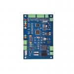
FR4 94V0 Circuit Board Diagram PCBA Electronics 12 Layer 16 Layer 18 Layer
|
|
Prototype Good Quality Electronics Multilayer PCBs Manufacture 94v0 Rohs Electronic Pcb&pcba
————————————————————————————————————————————————————— for your assemblies as needed. Using our own in-house Stock and MRP system which links to our production data we are able to manage Inventory levels, lead times and buffer stocks to meet your deadlines.
Specification of PCB Manufacturing
Lead time for Multilayer PCBs: Factory production lines:
FAQ Q1.What is needed for PCB PCBA quotation? A: PCB: Quantity, Gerber file and Fabrication requirements(material,surface finish treatment, copper thickness,board thickness ,...) PCBA: BOM list, Standard ,Function Testing Methods.
Q2. MOQ? A: There is no MOQ in CKS.We are able to handle Small as well as large volume production with flexibility.
Q3.Shipping cost? A: The shipping cost is determined by the destination, weight, packing size of the goods. Please let us know if you need us to quote you the shipping cost. Q4.Popular field? Smart Home; Medical Products; Smart Wearable ; Industrial Control
,IOT etc.
|
|||||||||||||||||||||||||||||||||||||||
| Product Tags: FR4 94V0 Circuit Board Diagram 94V0 Circuit Board Diagram PCBA 12L PCBA Electronics |

|
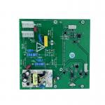
OEM SMT 4 Layer PCB 4mil 8 Layer PCB Manufacturer no MOQ |
|
IOT PCB PCBA 94V0 ROHS Multi Layer Circuit Board Sixteen Layer |
|
FR4 SHENGYI S1170 LED Aluminum Plate PCB Board IATF16949 RGB Circuit Board |
|
15W Qi Charging Coil And Circuit Board Multilayer PCBs HASL Lead Free |
|
Universal Miner board PCBA Security PCB Assembly 1-40L Multilayer Printed Circuit Board |
|
Turnkey PCBA 94V0 Fr4 Power Bank Charging Module Circuit Board |