
Laser Direct Imaging PCB With Scale Mode File Format For Application Of PCB HDI FPC
|
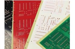
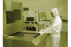
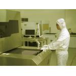
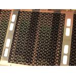
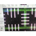
Laser Direct Imaging PCB With Scale Mode File Format For Application Of PCB HDI FPCProduct Description:Laser Direct Imaging (LDI) PCB combines the power of laser technology with direct imaging printing to create an efficient and effective PCB fabrication system. It is used for PCB, HDI and FPC applications. With a total power of 512W, the effective exposure area is up to 620x720mm, making it capable of handling a wide range of applications. The solder mask colors are customizable and can be set to fixed scale, auto scale, interval scale or partition alignment. The scale mode includes white, black, yellow and more. Additionally, the laser direct imaging printing board has excellent accuracy and repeatability, making it a reliable and cost-effective choice for PCB fabrication. Features:
Technical Parameters:
Applications:GIS DPX820SM Laser Direct Imaging PCB, a printed circuit board produced by Suzhou-based GIS, is the perfect choice for high-precision applications. It offers a file format with an ultra-precise ±12µm alignment accuracy, and a solder mask color with fixed scale/ auto scale/ interval scale/ partition alignment. With its laser power up to 512W and a board thickness ranging from 0.5 to 3.5mm, this Laser Direct Imaging Printed Circuit Board (Laser Direct Imaging Print Board) is ideal for applications requiring high precision. This Laser Direct Imaging PCB is perfect for the most demanding projects, and guarantees reliable and stable performance. Customization:GIS DPX820SM Laser Direct Imaging Printed Board This Laser Direct Imaging Circuit Board is made by GIS. It has a model number of DPX820SM, and is made in Suzhou, China. It has the following features:
This Laser Direct Imaging Printed Board is perfect for all your PCB, HDI, and FPC needs. The line width tolerance and effective exposure area are guaranteed, and the solder mask color can be customized to your exact specifications. Support and Services:Technical Support and Service for Laser Direct Imaging PCB At PCBWay, we provide technical support and service for our Laser Direct Imaging PCB products. Our team of experts are available to help you with any questions you may have about our products. We also provide product documentation, troubleshooting guides, and online tutorials that can help you get the most out of our Laser Direct Imaging PCB products. Our customer service team is available 24/7 to provide you with the best experience possible. Whether you have a technical issue or a general question, our team is here to help. We also offer a money back guarantee and free shipping on all our products. At PCBWay, we are committed to providing the best possible customer service and technical support for our Laser Direct Imaging PCB products. We are dedicated to making sure you have the best experience when using our products and are always looking for ways to improve our service. Packing and Shipping:Packaging and Shipping for Laser Direct Imaging PCB:
FAQ:Q1: What is Laser Direct Imaging PCB? Q2: What is the brand and model of the Laser Direct Imaging PCB? Q3: Where is the Laser Direct Imaging PCB manufactured? Q4: What are the advantages of using Laser Direct Imaging PCB? Q5: What materials are used to make Laser Direct Imaging PCB? |
||||||||||||||||||||||
| Product Tags: Scale Mode LDI Printed Board Laser Direct Imaging FPC Laser Direct Imaging FPC |
|
Laser Direct Imaging PCB With Scale Mode File Format For Application Of PCB HDI FPC |
|
380V Three Phase Laser Direct Imaging PCB HDI FPC |
|
FPC HDI 50um Laser Direct Imaging Equipment 610x710mm |
|
Laser Direct Imaging Printed Circuit Board With 30s@600x500mm Solder Mask Ink |
|
Laser Direct Imaging PCB Solder Mask For PCB、HDI、FPC With File Format |
|
File Format Laser Direct Imaging PCB With PAD Alignment Method 0.5~3.0mm Diameter |