
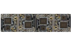
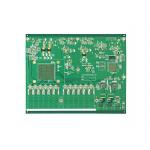
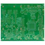
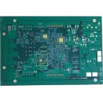
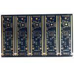
16 Layer Fpc Hdi Multilayer Pcb High Density Interconnect Boards 2.1mm
|
|
HDI stands for High Density Interconnector. It is a kind of printed circuit board that uses micro-blind buried hole technology to produce a circuit High Density Interconnector PCB board with High circuit distribution Density. HDI is a compact product designed for small volume users. HDI circuit advantages 1. Reduce PCB cost: When PCB density increases to more than eight layers, the cost of HDI manufacturing will be lower than the traditional complex pressing process. 2. Increase circuit density: traditional circuit board and parts interconnection 3. It is conducive to the use of advanced construction technology 4. Better electrical performance and signal correctness 5. Better reliability 6. Can improve the thermal properties 7. Can improve rf interference/electromagnetic interference/electrostatic release (RFI/EMI/ESD) 8. Increase design efficiency
FAQ: Q: What service do you have?
Q: What is needed for PCB & PCBA quotation?
Q: How to keep our product information and design file secret ?
Q: What are the main products of your PCB/PCBA services?
Q: What is your minimum order quantity (MOQ)?
Q: Are you factory? FASTPCB:Shangxing West Industrial Zone, Xihuan Road, Shajing Street, Bao 'an District, Shenzhen, Guangdong province, China |
||||||||||||||||||||||||||||||||||||||||||||||||||||||||||||||||||||||||||||||||||||||||||||||||||||||||||||||||||||||||||||||||||||||||||||||||||||||||||||||||||||||||||||||||||||||
| Product Tags: pcb fpc hdi 2.1mm 16 Layer Fpc Hdi Multilayer Pcbs 2.1mm high density interconnect printed circuit boards 2.1mm | ||||||||||||||||||||||||||||||||||||||||||||||||||||||||||||||||||||||||||||||||||||||||||||||||||||||||||||||||||||||||||||||||||||||||||||||||||||||||||||||||||||||||||||||||||||||
|
P1.65 Display Pcb Hdi Technology |
|
IPC High Density Interconnect Pcb Hdi Fr4 12 Layer |
|
Hdi Multilayer Pcb Wireless Router 1.6mm |
|
High Speed HDI PCB Board Small Hdi Pcb Prototype 18 Layer 3.2mm |
|
Twelve Layer 2 Step 6 Step HDI PCB Board Blind Buried Via Hole |
|
SBU HDI PCB Board BGA 2+6+2 3+4+3 Multilayer Layer |