
2 Layer Flex Pcb Printed Circuit Board Assembly Bonding
|
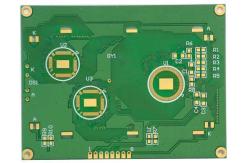
Double Sided Bonding Printed Circuit BoardThe Double Sided Bonding Printed Circuit Board is the rigidity PCB circuit board developed and produced by Shenzhen Quanhong Electronics Co., Ltd. the printed circuit board is made of FR-4 material, surface gold deposition and laser drilling. The minimum line width and line spacing can reach 75um and the minimum hole diameter can reach 0.1mm. The buried blind hole circuit board is widely used in digital cameras, notebooks, mobile phones and other electronic products and automotive electronics. Process capability
FAQ: Q: What service do you have?
Q: What is needed for PCB & PCBA quotation?
Q: How to keep our product information and design file secret ?
Q: What are the main products of your PCB/PCBA services?
Q: What is your minimum order quantity (MOQ)?
Q: Are you factory? FASTPCB:Shangxing West Industrial Zone, Xihuan Road, Shajing Street, Bao 'an District, Shenzhen, Guangdong province, China
|
|||||||||||||||||||||||||||||||||||||||||||||||||||||||||||||||||||||||||||||||||||||||||||||||||||||||||||||||||||||||||||||||||||||||||||||||||||||||||||||||||||||||||||||||||||||||||||||||||||||||||||||||||||||||||||||||||||||||||||||||||||||||||||||||||||||||||||||||||||||||||||||||||||||||
| Product Tags: 2 Layer Flex Pcb Printed Circuit Board Flex Pcb Printed Circuit Board Assembly 2 layer pcb board | |||||||||||||||||||||||||||||||||||||||||||||||||||||||||||||||||||||||||||||||||||||||||||||||||||||||||||||||||||||||||||||||||||||||||||||||||||||||||||||||||||||||||||||||||||||||||||||||||||||||||||||||||||||||||||||||||||||||||||||||||||||||||||||||||||||||||||||||||||||||||||||||||||||||
|
2.0mm 6L Red Purple Solder Mask Pcb Process For Communication Terminal |

|
1 OZ Copper Clad Laminate Pcb Printed Circuit Board Material Fr4 Pcb Assembly |
|
4.8mm 36 Layer Multi Layer Circuit Board Custom Pcb Printing |
|
1.6mm 0.5 Oz Copper Pcb Printed Circuit Board Company For Digital Security |
|
1/2 Oz Copper Prototype Pcb Printed Circuit Board Substrate For Mobile Phone |
|
Blue Black Soldermask PCB Industrial Equipment 6 Layer Copper Clad Fr4 Board |