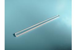
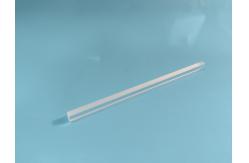
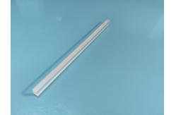
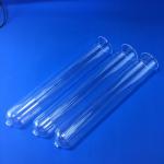
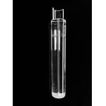
Sapphire Substrate 65x2.9x2mm Precision Polished Laser Equipment
Carrier Base
Product NameThe Sapphire Substrate is a precision thin strip component with a
dimension of 65 x 2.9 x 2mm, manufactured from single crystal
sapphire for demanding optical and laser applications. The
substrate is precision ground and polished to tight dimensional
tolerance, providing a flat, clean surface for mounting optical
elements and laser components. With no precipitation under
long-term high temperature service and excellent insulating
performance, the substrate maintains purity and stability in
extreme operating conditions. Its mechanical strength and wear
resistance are far superior to fused silica, making it a durable
choice for instrument windows, sensor bases and laser equipment
carriers.
Specification| Parameter | Specification |
|---|
| Dimension | 65 x 2.9 x 2mm |
| Material | Single crystal sapphire (alumina) |
| Surface Finish | Precision ground and polished |
| Tolerance | Tight dimensional tolerance |
| Insulation | Great insulating performance |
| Customization | Single/double side polishing, slotting, drilling, coating |
- Precision ground and polished thin strip: The long, thin blank is finished with high surface quality and
flatness for optical mounting.
- Tight dimensional tolerance: Length, width and thickness are controlled within narrow limits
for reliable assembly.
- No precipitation under long-term high temperature: The pure sapphire material releases no contaminants in
high-temperature service.
- Great insulating performance: Excellent electrical insulation supports use in sensitive
electronic and optical systems.
- Higher mechanical strength and wear resistance than fused silica: The tough substrate resists impact, wear and handling damage.
- Customizable processing: Single or double side polishing, slotting, drilling and coating
can be tailored to requirements.
ApplicationThe Sapphire Substrate is designed for optical, laser and sensing
systems that require a strong, stable and precisely dimensioned
platform. It is widely used as a precision optical instrument
window, providing a durable, transparent aperture for light
transmission. In laser systems, the substrate serves as a carrier
substrate for laser equipment, supporting components with excellent
thermal and mechanical stability. The component is also adopted as
a high-temperature inspection viewing plate, allowing observation
of processes at elevated temperatures. In sensing systems, it works
as a light-transmitting substrate for sensors, combining optical
clarity with electrical insulation. Additionally, the substrate is
used as an optical part for spectral analyzers, delivering
consistent performance across batches.
Advantages- Precision grinding and polishing for thin strip blanks: Tight dimensional tolerance ensures accurate fit in precision
assemblies.
- No precipitation and great insulation: Long-term high-temperature service keeps the substrate pure and
electrically safe.
- Superior mechanical strength and wear resistance: Far stronger than fused silica, the substrate resists scratches
and impact.
- Full customization: Polishing, slotting, drilling and coating processes are available
to match application needs.
- Consistent optical performance in mass production: Batch uniformity delivers repeatable results for volume
applications.