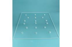
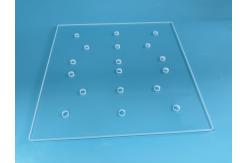
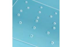
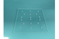
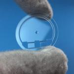
Thickened 9 inch Wafer Calibration quartz glass plate high
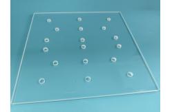
temperature Product NameThe Thickened 9-inch Wafer Calibration Glass Plate is a precision
optical reference substrate engineered for semiconductor wafer
dimension, appearance and flatness inspection. Manufactured from
high-transmittance fused silica or alkali-free borosilicate glass,
this calibration plate matches the standard 9-inch wafer dimension
while offering a customized thickened structure that resists
bending and warpage during repeated inspection cycles. The
double-sided ultra-precision polished surfaces deliver
optical-grade flatness and parallelism, providing a stable
geometric baseline for automated optical inspection systems. As a
dedicated calibration reference, the plate ensures that measurement
data remains consistent and repeatable across long production runs,
making it an essential tool for wafer fabrication, lithography
alignment and optical image measurement applications. Specification| Parameter | Specification |
|---|
| Size | 9-inch, matching standard wafer dimension | | Thickness | Customized thickened design | | Material | High-transmittance fused silica / alkali-free borosilicate glass
(optional) | | Surface Finish | Double-sided ultra-precision optical polishing | | Flatness & Parallelism | Optical reference grade | | Edge Treatment | Precision chamfered, chipping-free | | Application | Wafer dimension, appearance and flatness inspection |
- Thickened structure for rigidity: The reinforced plate avoids warpage and deformation during
inspection, delivering stable and repeatable calibration data.
- Double-sided ultra-precision optical polishing: Surfaces are free of scratches, pits, bubbles and stones, with
optical-grade flatness and parallelism.
- Uniform high transmittance from UV to visible light: The high-purity substrate minimizes stray light interference and
is fully compatible with AOI automatic optical inspection
equipment.
- Low thermal expansion coefficient: Minimal deformation under temperature change keeps the reference
geometry stable, and the material resists acid and alkali cleaning
solutions.
- Precision chamfered edges: Chipping-free edges protect wafers and inspection lenses from
scratches during handling and loading.
ApplicationThe Thickened 9-inch Wafer Calibration Glass Plate serves as a
versatile optical reference in semiconductor manufacturing and
inspection environments. It is widely used for 9-inch silicon wafer
dimension calibration, providing a trusted geometric standard that
verifies the accuracy of measurement tools. In wafer flatness
inspection, the optical-grade surface acts as a reliable reference
baseline for comparing surface uniformity and detecting deviation.
The plate also functions as a standard carrier for optical image
measuring instruments, supporting consistent positioning during
dimensional analysis. In lithography equipment, it works as an
alignment calibration plate that helps maintain precise pattern
registration. Additionally, the plate is adopted as a fixture base
for wafer surface defect inspection, offering a flat, stable and
contamination-free platform for automated defect detection systems. Advantages- Anti-bending thickened plate: The reinforced structure prevents reference offset during
long-term mass inspection, keeping calibration results reliable
shift after shift.
- High-purity material without precipitation: The clean substrate releases no contaminants, protecting wafers
from pollution during contact inspection.
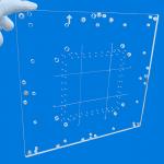
- Full customization available: Thickness, optical coating, alignment scale marking, slotting and
drilling can all be tailored to customer requirements.
- High single-piece consistency: Tight manufacturing control ensures the plates are interchangeable
across multiple inspection machines with identical performance.
|