
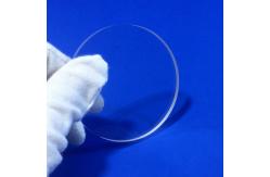
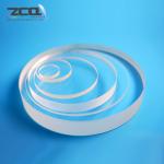
Quartz Glass Plate Semiconductor Fused Silica Wafer Quartz Glass
|
|
Semiconductor Fused Silica Quartz Glass wafer Specifications Process Shape Cut Thin sheets are scribed, thick sheets are water jetted and blocks are wire sawn to begin the process with a wafer "blank". CNC Edge Each wafer is individually edged on a Precision CNC Edge Grinding Station. Lapping As required, wafers are lapped to precise thickness or flatness. Polishing Double-side Commercial Polish removes subsurface damage and Super Polish creates a pristine finish. Cleaning We combine ultrasonics and megasonics on multiple cleaning lines which feed directly into a Class Clean Room. Inspection In our Class 100 Optical Clean Room, we inspect to various quality levels under the appropriate lighting conditions. Packaging All wafers are packed in pre-cleaned containers, double bagged and vacuum sealed within the Class 100 Clean Room. |
| Product Tags: semiconductor fused silica wafer quartz glass fused silica wafer fused silica semiconductor wafer |

|
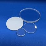
Quartz Glass Plate High Purity Size Can Be Customized |
|
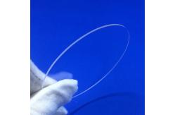
High Purity Quartz Pendulum Without Coating |
|
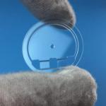
Custom Produced Perforated Machining Quartz Glass Plate High Temperature Resistant |
|
Optical Communication Quartz Glass Plate High Precision |
|
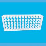
0.1mm Thickness Quartz Discs High Temperature Resistant Clear |
|
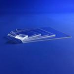
High Precision Smooth Quartz Glass Sheet In Optics Fields |