
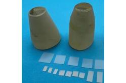
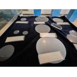
Polish Square Fe Doped SrTiO3 Crystal Wafer Optical Windows
|
|
10mm Square Fe Doped SrTiO3 Crystal Wafer Used As Optical Windows
SrTiO3 Crystal Wafer Description Nb doped strontium titanate (Nb:SrTiO3) has similar structure to strontium titanate single crystal, but Nb:SrTiO3 has electrical conductivity. The resistance of niobium-doped strontium titanate varies from 0.1-0.001W-cm with the concentration of niobium-doped 0.1-0.001wt%. The conductive single crystal substrate provides electrodes for the film and device.
SrTiO3 (Strontium Titanate) crystal wafer is a type of substrate made from single-crystal SrTiO3 material. SrTiO3 Crystal Wafer is used in the electronics and semiconductor industries as a substrate for thin film deposition and device fabrication.
SrTiO3 Crystal Wafer Details
SrTiO3 Crystal Wafer Application: Capacitors Field-Effect Transistors (FETs)
main products
|
||||||||||||||||||||||||||
| Product Tags: Square Fe Doped SrTiO3 Crystal Wafer Optical Windows Crystal Wafer Polish SrTiO3 Crystal Wafer | ||||||||||||||||||||||||||
|
Stoichiometric LiTaO3 Wafers Ideal Material for Optical Modulators and Frequency Converters |
|
3" 4" 6" Single Crystal Quartz With Customized Wafers And Their Outstanding Material Properties |
|
3" 4" 6"Single Crystal Quartz Wafers For High Temperature Applications Customized Orientation Options With 3 Inch And 4 Inch Sizes |
|
3 Inch And 4 InchCustomized Orientation Options For Single Crystal Quartz Wafer High Temperature |
|
Stoichiometric LiTaO3 Wafers The Ultimate Choice for High-Frequency Electronics |
|
2" 3" 4" 6" Lithium Tantalate Wafers Ultimate Solution For Piezoelectric Applications |