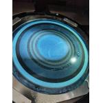
Semiconductor Sapphire Wafer Sapphire Windows Piezoelectric Wafer Sapphire is a material of a unique combination of physical,
chemical and optical properties, which make it resistant to high
temperature, thermal shock, water and sand erosion, and scratching.
It is a superior window material for many IR applications from 3µm
to 5µm. C-plane sapphire substrates are widely used to grow III-V
and II-VI compounds such as GaN for blue LED and laser diodes,
while R-plane sapphire substrates are used for the hetero-epitaxial
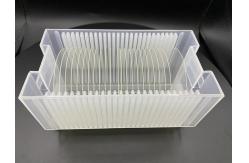
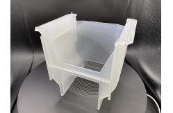
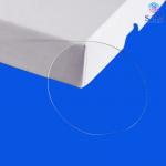
deposition of silicon for microelectronic IC applications. Item | 3-inch C-plane(0001) 500μm Sapphire Wafers | Crystal Materials | 99,999%, High Purity, Monocrystalline Al2O3 | Grade | Prime, Epi-Ready | Surface Orientation | C-plane(0001) | C-plane off-angle toward M-axis 0.2 +/- 0.1° | Diameter | 76.2 mm +/- 0.1 mm | Thickness | 500 μm +/- 25 μm | Primary Flat Orientation | A-plane(11-20) +/- 0.2° | Primary Flat Length | 22.0 mm +/- 1.0 mm | Single Side Polished | Front Surface | Epi-polished, Ra < 0.2 nm (by AFM) | (SSP) | Back Surface | Fine ground, Ra = 0.8 μm to 1.2 μm | Double Side Polished | Front Surface | Epi-polished, Ra < 0.2 nm (by AFM) | (DSP) | Back Surface | Epi-polished, Ra < 0.2 nm (by AFM) | TTV | < 15 μm | BOW | < 15 μm | WARP | < 15 μm | Cleaning / Packaging | Class 100 cleanroom cleaning and vacuum packaging, | 25 pieces in one cassette packaging or single piece packaging. |
Item | 4-inch C-plane(0001) 650μm Sapphire Wafers | Crystal Materials | 99,999%, High Purity, Monocrystalline Al2O3 | Grade | Prime, Epi-Ready | Surface Orientation | C-plane(0001) | C-plane off-angle toward M-axis 0.2 +/- 0.1° | Diameter | 100.0 mm +/- 0.1 mm | Thickness | 650 μm +/- 25 μm | Primary Flat Orientation | A-plane(11-20) +/- 0.2° | Primary Flat Length | 30.0 mm +/- 1.0 mm | Single Side Polished | Front Surface | Epi-polished, Ra < 0.2 nm (by AFM) | (SSP) | Back Surface | Fine ground, Ra = 0.8 μm to 1.2 μm | Double Side Polished | Front Surface | Epi-polished, Ra < 0.2 nm (by AFM) | (DSP) | Back Surface | Epi-polished, Ra < 0.2 nm (by AFM) | TTV | < 20 μm | BOW | < 20 μm | WARP | < 20 μm | Cleaning / Packaging | Class 100 cleanroom cleaning and vacuum packaging, | 25 pieces in one cassette packaging or single piece packaging. |
Item | 6-inch C-plane(0001) 1300μm Sapphire Wafers | Crystal Materials | 99,999%, High Purity, Monocrystalline Al2O3 | Grade | Prime, Epi-Ready | Surface Orientation | C-plane(0001) | C-plane off-angle toward M-axis 0.2 +/- 0.1° | Diameter | 150.0 mm +/- 0.2 mm | Thickness | 1300 μm +/- 25 μm | Primary Flat Orientation | A-plane(11-20) +/- 0.2° | Primary Flat Length | 47.0 mm +/- 1.0 mm | Single Side Polished | Front Surface | Epi-polished, Ra < 0.2 nm (by AFM) | (SSP) | Back Surface | Fine ground, Ra = 0.8 μm to 1.2 μm | Double Side Polished | Front Surface | Epi-polished, Ra < 0.2 nm (by AFM) | (DSP) | Back Surface | Epi-polished, Ra < 0.2 nm (by AFM) | TTV | < 25 μm | BOW | < 25 μm | WARP | < 25 μm | Cleaning / Packaging | Class 100 cleanroom cleaning and vacuum packaging, | 25 pieces in one cassette packaging or single piece packaging. |
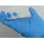
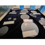
Acceptance Check
|