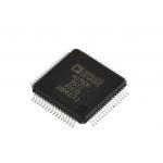
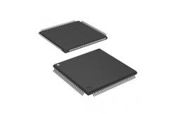
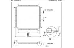
TMS320VC5409APGE16 Digital Signal Processor IC DSP Integrated Circuits QFP144
|
|
TMS320VC5409APGE16 Digital Signal Processors DSP Integrated Circuits QFP144 Texas Instruments ICs
Description:
The TMS320VC5409A fixed-point, digital signal processor (DSP)
(hereafter referred to as the 5409A
Specification:Fixed-Point Digital Signal Processor IC
Features: Advanced Multibus Architecture With Three Parallel Load Separate 16-Bit Data Memory Buses and One • Conditional Store Instructions Program Memory Bus • Fast Return From Interrupt • 40-Bit Arithmetic Logic Unit (ALU) Including a • On-Chip Peripherals 40-Bit Barrel Shifter and Two Independent – Software-Programmable Wait-State 40-Bit Accumulators Generator and Programmable • 17- × 17-Bit Parallel Multiplier Coupled to a Bank-Switching 40-Bit Dedicated Adder for Non-Pipelined – On-Chip Programmable Phase-Locked Single-Cycle Multiply/Accumulate (MAC) Loop (PLL) Clock Generator With Internal Operation Oscillator or External Clock Source(1) • Compare, Select, and Store Unit (CSSU) for the – One 16-Bit Timer Add/Compare Selection of the Viterbi Operator – Six-Channel Direct Memory Access (DMA) Controller • Exponent Encoder to Compute an Exponent Value of – Three Multichannel Buffered Serial Ports a 40-Bit Accumulator Value in a (McBSPs) Single Cycle – 8/16-Bit Enhanced Parallel Host-Port • Two Address Generators With Eight Auxiliary Interface (HPI8/16) Registers and Two Auxiliary Register • Power Consumption Control With IDLE1, Arithmetic Units (ARAUs) IDLE2, and IDLE3 Instructions With • Data Bus With a Bus Holder Feature Power-Down Modes • Extended Addressing Mode for 8M × 16-Bit • CLKOUT Off Control to Disable CLKOUT Maximum Addressable External Program • On-Chip Scan-Based Emulation Logic, IEEE Space Std 1149.1 (JTAG) Boundary Scan Logic (2) • 32K × 16-Bit On-Chip RAM Composed of: • 144-Pin Ball Grid Array (BGA) (GGU Suffix) – Four Blocks of 8K × 16-Bit On-Chip Dual-Access Program/Data RAM • 144-Pin Low-Profile Quad Flatpack (LQFP) (PGE Suffix) • 16K × 16-Bit On-Chip ROM Configured for Program Memory • 6.25-ns Single-Cycle Fixed-Point Instruction Execution Time (160 MIPS) • Enhanced External Parallel Interface (XIO2) • 8.33-ns Single-Cycle Fixed-Point Instruction • Single-Instruction-Repeat and Block-Repeat Operations Execution Time (120 MIPS) for Program Code • 3.3-V I/O Supply Voltage (160 and 120 MIPS) • Block-Memory-Move Instructions for Better Program and Data Management • 1.6-V Core Supply Voltage (160 MIPS) • Instructions With a 32-Bit Long Word Operand • 1.5-V Core Supply Voltage (120 MIPS) (1) The on-chip oscillator is not available on all 5409A devices.
Related products:
DEVICE OPTION PACKAGE FREQUENCY RATED CURRENT OUTPUT VOLTAGE LMR33630ADDA DDA (8-pin HSOIC) 5 × 4 mm 400 kHz 3 A LMR33630BDDA 1400 kHz 3 A Adjustable LMR33630CDDA 2100 kHz 3 A LMR33630ARNX RNX (12-pin VQFN) 3 × 2 × 0.85 mm 400 kHz 3 A LMR33630BRNX 1400 kHz 3 A Adjustable LMR33630CRNX 2100 kHz 3 A
All dimensions are nominal Device Package Type Package Drawing Pins SPQ Length (mm) Width (mm) Height (mm) LMR33630ADDAR SO PowerPAD DDA 8 2500 366.0 364.0 50.0 LMR33630ARNXR VQFN-HR RNX 12 3000 213.0 191.0 35.0 LMR33630ARNXR VQFN-HR RNX 12 3000 210.0 185.0 35.0 LMR33630ARNXT VQFN-HR RNX 12 250 210.0 185.0 35.0 LMR33630ARNXT VQFN-HR RNX 12 250 213.0 191.0 35.0 LMR33630BDDAR SO PowerPAD DDA 8 2500 366.0 364.0 50.0 LMR33630BRNXR VQFN-HR RNX 12 3000 213.0 191.0 35.0 LMR33630BRNXR VQFN-HR RNX 12 3000 210.0 185.0 35.0 LMR33630BRNXT VQFN-HR RNX 12 250 213.0 191.0 35.0 LMR33630BRNXT VQFN-HR RNX 12 250 210.0 185.0 35.0 LMR33630CDDAR SO PowerPAD DDA 8 2500 366.0 364.0 50.0 LMR33630CRNXR VQFN-HR RNX 12 3000 213.0 191.0 35.0 LMR33630CRNXR VQFN-HR RNX 12 3000 210.0 185.0 35.0 LMR33630CRNXT VQFN-HR RNX 12 250 210.0 185.0 35.0 LMR33630CRNXT VQFN-HR RNX 12 250 213.0 191.0 35.0
|
||||||||||||||||||||||||||||||||||||||
| Product Tags: TMS320VC5409APGE16 DSP Integrated Circuits QFP144 TMS320VC5409APGE16 Digital Signal Processor |