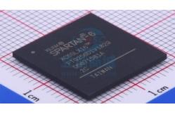
General Description
The Spartan®-6 family provides leading system integration
capabilities with the lowest total cost for high-volume
applications. The thirteen-member family delivers expanded
densities ranging from 3,840 to 147,443 logic cells, with half the
power consumption of previous Spartan families, and faster, more
comprehensive connectivity. Built on a mature 45 nm low-power
copper process technology that delivers the optimal balance of
cost, power, and performance, the Spartan-6 family offers a new,
more efficient, dual-register 6-input lookup table (LUT) logic and
a rich selection of built-in system-level blocks. These include 18
Kb (2 x 9 Kb) block RAMs, second generation DSP48A1 slices, SDRAM
memory controllers, enhanced mixed-mode clock management blocks,
SelectIO™ technology, poweroptimized high-speed serial transceiver
blocks, PCI Express® compatible Endpoint blocks, advanced
system-level power management modes, auto-detect configuration
options, and enhanced IP security with AES and Device DNA
protection. These features provide a lowcost programmable
alternative to custom ASIC products with unprecedented ease of use.
Spartan-6 FPGAs offer the best solution for high-volume logic
designs, consumer-oriented DSP designs, and cost-sensitive embedded
applications. Spartan-6 FPGAs are the programmable silicon
foundation for Targeted Design Platforms that deliver integrated
software and hardware components that enable designers to focus on
innovation as soon as their development cycle begins. Summary of
Spartan-6 FPGA Features
• Spartan-6 Family: • Spartan-6 LX FPGA: Logic optimized •
Spartan-6 LXT FPGA: High-speed serial connectivity • Designed for
low cost • Multiple efficient integrated blocks • Optimized
selection of I/O standards • Staggered pads • High-volume plastic
wire-bonded packages • Low static and dynamic power • 45 nm process
optimized for cost and low power • Hibernate power-down mode for
zero power • Suspend mode maintains state and configuration with
multi-pin wake-up, control enhancement • Lower-power 1.0V core
voltage (LX FPGAs, -1L only) • High performance 1.2V core voltage
(LX and LXT FPGAs, -2, -3, and -3N speed grades) • Multi-voltage,
multi-standard SelectIO™ interface banks • Up to 1,080 Mb/s data
transfer rate per differential I/O • Selectable output drive, up to
24 mA per pin • 3.3V to 1.2V I/O standards and protocols • Low-cost
HSTL and SSTL memory interfaces • Hot swap compliance • Adjustable
I/O slew rates to improve signal integrity • High-speed GTP serial
transceivers in the LXT FPGAs • Up to 3.2 Gb/s • High-speed
interfaces including: Serial ATA, Aurora, 1G Ethernet, PCI Express,
OBSAI, CPRI, EPON, GPON, DisplayPort, and XAUI • Integrated
Endpoint block for PCI Express designs (LXT) • Low-cost PCI®
technology support compatible with the 33 MHz, 32- and 64-bit
specification. • Efficient DSP48A1 slices • High-performance
arithmetic and signal processing • Fast 18 x 18 multiplier and
48-bit accumulator • Pipelining and cascading capability •
Pre-adder to assist filter applications • Integrated Memory
Controller blocks • DDR, DDR2, DDR3, and LPDDR support • Data rates
up to 800 Mb/s (12.8 Gb/s peak bandwidth) • Multi-port bus
structure with independent FIFO to reduce design timing issues •
Abundant logic resources with increased logic capacity • Optional
shift register or distributed RAM support • Efficient 6-input LUTs
improve performance and minimize power • LUT with dual flip-flops
for pipeline centric applications • Block RAM with a wide range of
granularity • Fast block RAM with byte write enable • 18 Kb blocks
that can be optionally programmed as two independent 9 Kb block
RAMs • Clock Management Tile (CMT) for enhanced performance • Low
noise, flexible clocking • Digital Clock Managers (DCMs) eliminate
clock skew and duty cycle distortion • Phase-Locked Loops (PLLs)
for low-jitter clocking • Frequency synthesis with simultaneous
multiplication, division, and phase shifting • Sixteen low-skew
global clock networks • Simplified configuration, supports low-cost
standards • 2-pin auto-detect configuration • Broad third-party SPI
(up to x4) and NOR flash support • Feature rich Xilinx Platform
Flash with JTAG • MultiBoot support for remote upgrade with
multiple bitstreams, using watchdog protection • Enhanced security
for design protection • Unique Device DNA identifier for design
authentication • AES bitstream encryption in the larger devices •
Faster embedded processing with enhanced, low cost, MicroBlaze™
soft processor • Industry-leading IP and reference designs