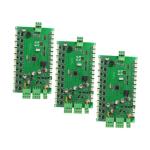
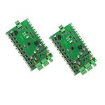
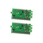
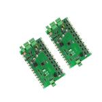
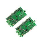
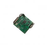
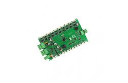
Multi-Layer Boards PCB Assembly Services Producibility Carbon Ink
Nelco PCB Assembly Services Description: 1. Focus on component sourcing.
2. Management team with 10+ years of experience in the material.
3. PCB Component Sourcing Teams: Project department, Engineering
department, Purchasing.
4. department, Quality department, Customs Declaration department.
5. Professional component validation engineers.
6. Professional BOM Engineers.
PCB Assembly Services Parameters:
Item | Technical Parameter | Layer | 2-64 | Thickness | 0.5-17.5mm | Copper Thickness | 0.3-12 oz | Min Mechanical Hole | 0.1mm | Min Laser Hole | 0.075mm | HDI | 1+n+1,2+n+2,3+n+3 | Max Aspect Ratio | 20:01 | Max Board Size | 650mm*1130mm | Min Width/Space | 2.4/2.4mil | Min Outline Tolerance | ±0.1mm | Impedance Tolerance | ±5% | Min PP Thickness | 0.06mm | Bow &Twist | ≤0.5% | Materials | FR4,High-Tg FR4,Rogers, Nelco,RCC,PTFE, M4, M6,TU862,TU872 | Surface Finished | HASL, HASL Pb Free Immersion Gold/Tin/Silver Osp, Immersion
Gold+OSP | Special Capability | Gold Finger Plating, Peelable, Carbon ink |
PCB Assembly Services Introduction: The creator of PCB is the Austrian Paul Eisler, who first used
printed circuit boards in radios in 1936. In 1943, Americans mostly
used this technology in military radios, and in 1948, the United
States officially recognized this invention for commercial use.
Printed circuit boards have only been widely used since the
mid-1950s. Printed circuit boards are found in almost every
electronic device. If there are electronic parts in a device, they
are all mounted on PCBs of various sizes. The main function of the
PCB is to make various electronic components form the connection of
the predetermined circuit, which plays the role of relay
transmission. It is the key electronic interconnection of
electronic products and is known as the "mother of electronic
products". |
