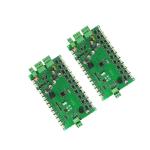
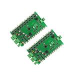
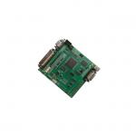
PCB Assembly Services Flexible Boards High-Reliability Gold Finger
Plating PCB Assembly Services Description: 1. Focus on component sourcing.
2. Management team with 10+ years of experience in the material.
3. PCB Component Sourcing Teams: Project department, Engineering
department, Purchasing.
4. department, Quality department, Customs Declaration department.
5. Professional component validation engineers.
6. Professional BOM Engineers.
PCB Assembly Services Parameters:
Item | Technical Parameter | Layer | 2-64 | Thickness | 0.5-17.5mm | Copper Thickness | 0.3-12 oz | Min Mechanical Hole | 0.1mm | Min Laser Hole | 0.075mm | HDI | 1+n+1,2+n+2,3+n+3 | Max Aspect Ratio | 20:01 | Max Board Size | 650mm*1130mm | Min Width/Space | 2.4/2.4mil | Min Outline Tolerance | ±0.1mm | Impedance Tolerance | ±5% | Min PP Thickness | 0.06mm | Bow &Twist | ≤0.5% | Materials | FR4,High-Tg FR4,Rogers, Nelco,RCC,PTFE, M4, M6,TU862,TU872 | Surface Finished | HASL, HASL Pb Free Immersion Gold/Tin/Silver Osp, Immersion
Gold+OSP | Special Capability | Gold Finger Plating, Peelable, Carbon ink |
PCB Assembly Services Introduction: The earliest use of printed circuit boards is paper-based
copper-clad printed boards. Since the advent of semiconductor
transistors in the 1950s, the demand for printed boards has risen
sharply. Especially with the rapid development and wide application
of integrated circuits, the volume of electronic equipment is
getting smaller and smaller, and the circuit wiring density and
difficulty are getting bigger and bigger, which requires the
printed board to be updated continuously. At present, the variety
of printed boards has developed from single-sided to double-sided,
multi-layer boards and flexible boards; the structure and quality
have also developed to ultra-high density, miniaturization, and
high reliability.
|