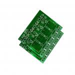
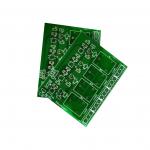
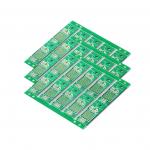
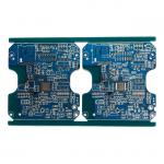
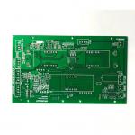
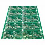
Quick Turn To Prototype Printed Circuit Board Fabrication TU862 POP
Board
Printed Circuit Board Fabrication Description:
1. A team of experts with more than 10 years of experience.
2. Professional component certified engineers and experienced
supply chain management team.
3. Pay attention to the latest international market information and
provide competitive prices.
4. Certified suppliers and parts.
Printed Circuit Board Fabrication Parameters:
| Item | Technical Parameter |
| Layer | 2-64 |
| Thickness | 0.3-6.5mm |
| Copper Thickness | 0.3-12 oz |
| Min Mechanical Hole | 0.1mm |
| Min Laser Hole | 0.075mm |
| HDI | 1+n+1,2+n+2,3+n+3 |
| Max Aspect Ratio | 20:01 |
| Max Board Size | 650mm*1130mm |
| Min Width/Space | 2.4/2.4mil |
| Min Outline Tolerance | ±0.1mm |
| Impedance Tolerance | ±5% |
| Min PP Thickness | 0.06mm |
| Bow &Twist | ≤0.5% |
| Materials | FR4, High-Tg FR4, Rogers, Nelco, RCC, PTFE, M4, M6, TU862, TU872 |
| Surface Finished | HASL, HASL Pb Free Immersion Gold/Tin/Silver Osp, Immersion
Gold+OSP |
| Special Capability | Gold Finger Plating, Peelable, Carbon ink |
FAQ:
Q. What is your Minimum Order Quantity (MOQ)?
There is no limit to our MOQ, depending on the specific
requirements, samples and mass production can be supported, and
customized models are supported.
Q: What are the payment terms we can accept?
We recommend that you use T/T, and other needs can be communicated
with our staff.
Printed Circuit Board Fabrication Introduction:
1. Provide the required electrical characteristics, characteristic
impedance, and electromagnetic compatibility characteristics for
the circuit in high-speed or high-frequency circuits.
2. The printed board with passive components embedded inside
provides certain electrical functions, simplifies the electronic
installation procedure, and improves the reliability of the
product.
3. In large-scale and ultra-large-scale electronic packaging
components, an effective chip carrier is provided for the
miniaturized chip packaging of electronic components.
