
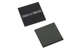
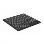
15360KB Flash LFMXO5-25-7BBG256C MachXO5-NX Field Programmable Gate Array Chip
|
|
15360KB Flash LFMXO5-25-7BBG256C MachXO5-NX Field Programmable Gate Array Chip
Product Description Of LFMXO5-25-7BBG256C LFMXO5-25-7BBG256C utilizes different components/resources for the transmit and receive paths of SGMII. For the SGMII transmit path, Generic DDR I/O with X5 gearing are used. The two hardened blocks are located at the bottom left of the chip and uses the high speed I/O Bank 5 for the differential pair input. It is recommended that the reference clock should be entered through a GPIO that has connection to the PLL on the lower left corner as well.
Product Attributes Of LFMXO5-25-7BBG256C
Features Of LFMXO5-25-7BBG256C
SGMII CDR IP Of LFMXO5-25-7BBG256C
FAQ |
|
Field Programmable Gate Array XCZU11EG-2FFVC1156E System On Chip FCBGA1156 SoC FPGA |

|
Field Programmable Gate Array XCZU9CG-2FFVB1156E 599K Logic Cells System On Chip |
|
Field Programmable Gate Array XCZU5EV-1FBVB900E 3.5 Mbit Embedded System On Chip FPGA IC |
|
Field Programmable Gate Array XC7VX690T-1FFG1927C FCBGA-1927 High-Performance FPGAs |
|
Field Programmable Gate Array XCKU115-1FLVA2104C High-Performance Kintex UltraScale FPGAs |
|
Field Programmable Gate Array LFE5UM5G-25F-8BG381I 400MHz FPGA Logic IC CABGA-381 |