
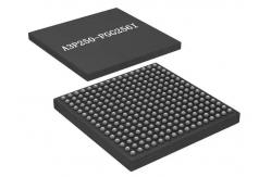
High Performance A3P250-FGG256I Low Power Programmable Logic IC 256-LBGA Package
|
|
High Performance A3P250-FGG256I Low Power Programmable Logic IC 256-LBGA Package
Product Description Of A3P250-FGG256I A3P250-FGG256I devices support the ARM Cortex-M1 processor.The ARM-enabled devices have Microchip ordering numbers that begin with M1A3P (Cortex-M1) and do not support AES decryption.A3P250-FGG256I have no PLL or RAM support.ProASIC 3 devices have up to 1 million system gates,supported with up to 144 kbits of true dual-port SRAM and up to 300 user I/Os.
Product Attributes Of A3P250-FGG256I
Feature Of A3P250-FGG256I
Output Buffer Model And Delays Of A3P250-FGG256I
FAQ |
|
Field Programmable Gate Array 5M160ZM100C5N 1.89V Complex Programmable Logic Devices |
|
Field Programmable Gate Array XC6SLX16-N3CPG196I Spartan-6 LX Embedded Field Programmable Gate Array IC |

|
Field Programmable Gate Array XC7S25-L1CSGA324I High Performance Spartan-7 Field Programmable Gate Array IC |

|
Field Programmable Gate Array XC7A15T-2CPG236C 106 I/O 6.25 Gb/s Artix-7 Field Programmable Gate Array IC |
|
Field Programmable Gate Array XC7A15T-1CPG236I 1V Artix-7 1.05V Field Programmable Gate Array IC 238-LFBGA |
|
Field Programmable Gate Array XC7A15T-L2FTG256E 0.95V High Performance 170 I/O Embedded Field Programmable Gate Array IC |