
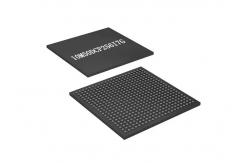
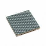
10M50DCF256I7G High Bandwidth Low Latency Field Programmable Gate Array
|
|
10M50DCF256I7G High Bandwidth Low Latency Field Programmable Gate Array
Product Description Of 10M50DCF256I7G 10M50DCF256I7G's eSRAM blocks is a new innovation. These large embedded SRAM blocks are tightly coupled to the core fabric and are directly accessible with no need for a separate memory controller. Each eSRAM block is arranged as 8 channels, 40 banks per channel, with a total capacity of 47.25 Mbits running at clock rates up to 750 MHz. Within the eSRAM block,each channel has a bus width of 72 bit read and 72 bit write, and has one READ and one WRITE per channel. This allows each eSRAM block to support a total aggregate bandwidth (read + write) of up to 864 Gbps.
Product Attributes Of 10M50DCF256I7G
Features Of 10M50DCF256I7G
Hard Memory Controller Of 10M50DCF256I7G
FAQ |

|
Integrated Circuit Chip EP4CE6F17C8N Embedded Field Programmable Gate Array 256-LBGA |
|
Field Programmable Gate Array XC7VX690T-1FFG1926I FPGA IC 1.2V To 3.3V Virtex-7 FPGAs |
|
Field Programmable Gate Array XCKU085-1FLVF1924I Kintex UltraScale FPGAs FBGA-1924 |
|
Field Programmable Gate Array XCKU115-3FLVA1517E Kintex UltraScale FPGAs FBGA-1517 |
|
Field Programmable Gate Array XCKU035-1SFVA784I Kintex UltraScale FPGA Chip BFBGA784 |

|
Field Programmable Gate Array 5ASXFB3G6F35C6G 1.05GHz ARM Cortex-A9 Embedded FPGA IC |