
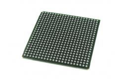
MAX 10 FPGA 10M50DCF484C7G Field Programmable Gate Array IC 484-FBGA Package
|
|
MAX 10 FPGA 10M50DCF484C7G Field Programmable Gate Array IC 484-FBGA Package
Product Description Of 10M50DCF484C7G 10M50DCF484C7G FPGAs feature power-efficient, dual-mode transceivers, capable of both 57.8 Gbps PAM4 (Pulse Amplitude Modulation) and 28.9 Gbps NRZ (Non Return to Zero) operation. 10M50DCF484C7G Supported by hardened PCI Express Gen 3 and 10/25/100 Gbps Ethernet MAC IP blocks, these devices can deliver over 8 Tbps of aggregate bandwidth, meeting the demanding transceiver bandwidth and power budget specifications of next generation designs.
Specification Of 10M50DCF484C7G
Features Of 10M50DCF484C7G
Standard Voltage Diagram Of 10M50DCF484C7G
FAQ |
|
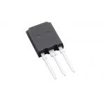
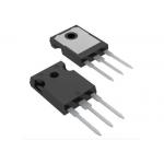
IGBT Trench Field Stop Transistors IKQ75N120CS7XKSA1 Integrated Circuit Chip |
|
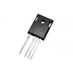
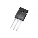
IKY50N120CH7XKSA1 IGBT Trench Field Stop 1200 V 75 A IGBTs Transistors |
|
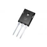
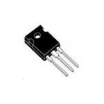
Single IGBTs Transistors IKW40N120CH7XKSA1 TO-247-3 IGBT Trench Field Stop 1200V |
|
IGBT Transistors 650V 40A 136W IKW20N65ET7XKSA1 Integrated Circuit Chip |
|
1200V IGBT Transistors IKW40N120CS7XKSA1 357W IGBT Trench Field Stop TO-247-3 |
|
Electronic Integrated Circuits IKW30N65ET7XKSA1 IGBT Trench Field Stop Transistors |