
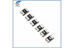
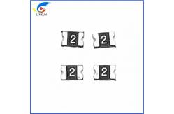
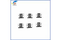
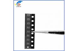
Silkscreen JK-SMD0805-110 6V1.1A PPTC Chip Resettable Fuse Selection
|
|
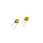
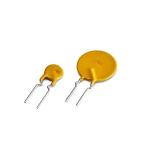
Surface Mountable PTC Resettable Fuse: JK-SMD0805 Series
Features:
Product Dimensions Terminal pad materials :Tin-Plated Nickle-copper Terminal pad solderability : Meets EIA specification RS 186-9E and ANSI/J-STD-002 Category 3. Unit :mm
Thermal Derating Chart-IH(A)
Electrical Characteristic
Test Procedures And Requirements
Physical Characteristics and Environmental Specifications Physical Characteristics
Electrical Specifications: Ihold = Hold Current. Maximum current device will not trip in 25°C still air. Itrip = Trip Current. Minimum current at which the device will always trip in 25°C still air. Vmax = Maximum operating voltage device can withstand without damage at rated current (Imax). Imax = Maximum fault current device can withstand without damage at rated voltage (Vmax). Pd=Maximum power dissipation when device is in the tripped state in 25°C still air environment at rated voltage. Rimin/max = Minimum/Maximum device resistance prior to tripping at 25°C. R1max = Maximum device resistance is measured one hour post reflow.
Recommended pad layout (mm) Solder reflow conditions Recommended reflow methods: IR, vapor phase oven, hot air oven, N2 environment for lead-free. ● Devices are not designed to be wave soldered to the bottom side of the board. ● Recommended maximum paste thickness is 0.25mm (0.010inch). ● Devices can be cleaned using standard industry methods and solvents. ● Soldering temprature profile meets RoHsleadfree process. Notes: If reflow temperatures exceed the recommended profile, devices may not meet the performance requirements
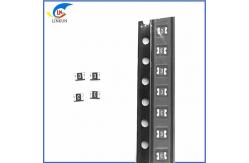
Tape Specification And Reel Dimensions
Packaging Quantity
Storage The maximum ambient temperature shall not exceed 38℃. Storage temperatures higher than 38℃ could result in the deformation of packaging materials. The maximum relative humidity recommended for storage is 60%. High humidity with high temperature can accelerate the oxidation of the solder plating on the termination and reduce the solderability of the components. Sealed plastic bags with desiccant shall be used to reduce the oxidation of the termination and shall only be opened prior to use. The products shall not be stored in areas where harmful gases containing sulfur or chlorine are present WARNING • Use PPTC beyond the maximum ratings or improper use may result in device damage and possible electrical arcing and flame. • PPTC are intended for protection against occasional over current or over temperature fault conditions and should not be used when repeated fault conditions or prolonged trip events are anticipated. • Device performance can be impacted negatively if devices are handled in a manner inconsistent with recommended electronic, thermal, and mechanical procedures for electronic components. • Use PPTC with a large inductance in circuit will generate a circuit voltage (L di/dt) above the rated voltage of the PPTC. • Avoid impact PPTC device its thermal expansion like placed under pressure or installed in limited space. • Contamination of the PPTC material with certain silicon based oils or some aggressive solvents can adversely impact the performance of the devices.PPTC SMD can be cleaned by standard methods. • Requests that customers comply with our recommended solder pad layouts and recommended reflow profile. Improper board layouts or reflow profilecould negatively impact solderability performance of our devices. Notes
The specification is intended to present application,product and technical data to assist the user in selecting PPTC circuit production devices,However,users should imdependently evaluate and test the suitability of each product.JinRui makes on warranties as to the acduracy or completeness of the information and disclaims any liatility resulting form its use,JinRui’s only obligations are those im the JinRui Standard Rerms and Conditions of Sale and in no case will JinRui be liable for any incidental,imdirect,or consequential damages arising from the sale,resale,ormisues of its products.Jinrui reserves the right to change of update,without notice,any information contained in this specification.
|
|||||||||||||||||||||||||||||||||||||||||||||||||||||||||||||||||||||||||||||||||||||||||||||||||||||||||||||||||||||||||||||||||||||||||||||||||||||||||||||||||||||||||||||||||||||||||||||||||||||||||||||||||||||||||||||||||||||||||||||||||||||||||||||||||||||||||||||||||||||||||||||||||||||||||||||||||||||||||||||||||||||||||||||||||||||||||||||||||||||||||||||||||||||||||||||||||||||||||||||||||||||||||||||||||||||||||||||||||||||||||||||||||||||||||||||||||||||||||||||||||||||||||||||||||||||||||||||||||||||||||||||||||||||||||||||||||||||||||||||||||||||||||||||||||||||||||||||||||||||||||||||||||||||||||||||||||||||||||||||||||||||||||||||||||||||||||||||||||||||||||||||||||||||||||||||||||||||||||||||||||||
| Product Tags: PPTC Chip Resettable Fuse PPTC Chip Resettable Fuse Silkscreen PPTC Chip Resettable Fuse | |||||||||||||||||||||||||||||||||||||||||||||||||||||||||||||||||||||||||||||||||||||||||||||||||||||||||||||||||||||||||||||||||||||||||||||||||||||||||||||||||||||||||||||||||||||||||||||||||||||||||||||||||||||||||||||||||||||||||||||||||||||||||||||||||||||||||||||||||||||||||||||||||||||||||||||||||||||||||||||||||||||||||||||||||||||||||||||||||||||||||||||||||||||||||||||||||||||||||||||||||||||||||||||||||||||||||||||||||||||||||||||||||||||||||||||||||||||||||||||||||||||||||||||||||||||||||||||||||||||||||||||||||||||||||||||||||||||||||||||||||||||||||||||||||||||||||||||||||||||||||||||||||||||||||||||||||||||||||||||||||||||||||||||||||||||||||||||||||||||||||||||||||||||||||||||||||||||||||||||||||||
|
Household Stable PPTC Thermistor UL94 V-0 Insulating Material |
|
High Molecule Polymer PPTC Thermistor Practical Resettable Fuse |
|
CE Lead Free PPTC Thermistor Multipurpose For Motor Overload |
|
Heat Resistance PPTC Thermistor Stable Performance Practical |
|
Durable Polymeric PPTC Thermistor Lightweight Lead Free Low Resistance |
|
UL Stable PPTC Resettable Fuse , Polymer Positive Temperature Coefficient Thermistor |