
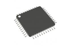
PIC18LF4520I/PT Electronic Integrated Circuit Components Enhanced Flash Microcontrollers
|
|
PIC18F2420/2520/4420/4520
28/40/44-Pin Enhanced Flash Microcontrollers with 10-Bit A/D and nanoWatt Technology
Power Managed Modes: • Run: CPU on, peripherals on • Idle: CPU off, peripherals on • Sleep: CPU off, peripherals off • Idle mode currents down to 5.8 µA typical • Sleep mode current down to 0.1 µA typical • Timer1 Oscillator: 1.8 µA, 32 kHz, 2V • Watchdog Timer: 2.1 µA • Two-Speed Oscillator Start-up
Peripheral Highlights: • High-current sink/source 25 mA/25 mA • Three programmable external interrupts • Four input change interrupts • Up to 2 Capture/Compare/PWM (CCP) modules, one with Auto-Shutdown (28-pin devices) • Enhanced Capture/Compare/PWM (ECCP) module (40/44-pin devices only): - One, two or four PWM outputs - Selectable polarity - Programmable dead time - Auto-Shutdown and Auto-Restart
• Master Synchronous Serial Port (MSSP) module supporting 3-wire SPI™ (all 4 modes) and I2C™ Master and Slave Modes • Enhanced Addressable USART module: - Supports RS-485, RS-232 and LIN 1.2 - RS-232 operation using internal oscillator block (no external crystal required) - Auto-Wake-up on Start bit - Auto-Baud Detect • 10-bit, up to 13-channel Analog-to-Digital Converter module (A/D): - Auto-acquisition capability - Conversion available during Sleep • Dual analog comparators with input multiplexing)
Flexible Oscillator Structure: • Four Crystal modes, up to 40 MHz • 4X Phase Lock Loop (available for crystal and internal oscillators) • Two External RC modes, up to 4 MHz • Two External Clock modes, up to 40 MHz • Internal oscillator block: - 8 user selectable frequencies, from 31 kHz to 8 MHz - Provides a complete range of clock speeds from 31 kHz to 32 MHz when used with PLL - User tunable to compensate for frequency drift • Secondary oscillator using Timer1 @ 32 kHz • Fail-Safe Clock Monitor: - Allows for safe shutdown if peripheral clock stops
Special Microcontroller Features: • C compiler optimized architecture: - Optional extended instruction set designed to optimize re-entrant code • 100,000 erase/write cycle Enhanced Flash program memory typical • 1,000,000 erase/write cycle Data EEPROM memory typical • Flash/Data EEPROM Retention: 100 years typical • Self-programmable under software control • Priority levels for interrupts • 8 x 8 Single-Cycle Hardware Multiplier
• Extended Watchdog Timer (WDT): - Programmable period from 4 ms to 131s • Single-supply 5V In-Circuit Serial Programming™ (ICSP™) via two pins • In-Circuit Debug (ICD) via two pins • Wide operating voltage range: 2.0V to 5.5V • Programmable 16-level High/Low-Voltage Detection (HLVD) module: - Supports interrupt on High/Low-Voltage Detection • Programmable Brown-out Reset (BOR - With software enable option
Absolute Maximum Ratings (†)
Ambient temperature under bias...........................................................................-40°C to +125°C Storage temperature ........................................................................................... -65°C to +150°C Voltage on any pin with respect to VSS (except VDD, MCLR and RA4) ........ -0.3V to (VDD + 0.3V) Voltage on VDD with respect to VSS ........................................................................ -0.3V to +7.5V Voltage on MCLR with respect to VSS (Note 2) ........................................................ 0V to +13.25V
Total power dissipation (Note 1) ..............................................................................................1.0W Maximum current out of VSS pin ...........................................................................................300 mA Maximum current into VDD pin ..............................................................................................250 mA Input clamp current, IIK (VI < 0 or VI > VDD).......................................................................... ±20 mA Output clamp current, IOK (VO < 0 or VO > VDD) .................................................................. ±20 mA
Maximum output current sunk by any I/O pin............................................................................25 mA Maximum output current sourced by any I/O pin ......................................................................25 mA Maximum current sunk by all ports .........................................................................................200 mA Maximum current sourced by all ports ....................................................................................200 mA
Note 1: Power dissipation is calculated as follows: Pdis = VDD x {IDD – ∑ IOH} + ∑ {(VDD – VOH) x IOH} + ∑(VOL x IOL) 2: Voltage spikes below VSS at the MCLR/VPP/RE3 pin, inducing currents greater than 80 mA, may cause latch-up. Thus, a series resistor of 50-100Ω should be used when applying a “low” level to the MCLR/VPP/ RE3 pin, rather than pulling this pin directly to VSS.
† NOTICE: Stresses above those listed under “Absolute Maximum Ratings” may cause permanent damage to the device. This is a stress rating only and functional operation of the device at those or any other conditions above those indicated in the operation listings of this specification is not implied. Exposure to maximum rating conditions for extended periods may affect device reliability.
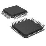
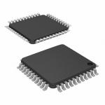
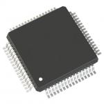
Pin Diagrams
Stock Offer (Hot Sell)
|
|||||||||||||||||||||||||||||||||||||||||||||||||||||||||||||||||||||||||||||||||||||||||||||||||||||||||||||||||||||||||||||||||||||||||||||||||||||||||||
| Product Tags: electronic integrated circuit linear integrated circuits |
|
AT89C2051-24PU Electronic IC Chip NEW AND ORIGINAL STOCK |
|
MC9S08GT32ACFBE Flash Memory IC NEW AND ORIGINAL STOCK |
|
MC9S08AC60CFGE Flash Memory IC NEW AND ORIGINAL STOCK |

|
MC9S08AW32CFGE Flash Memory IC NEW AND ORIGINAL STOCK |
|
MC9S08AW32CPUE Flash Memory IC NEW AND ORIGINAL STOCK |
|
MC68332GCAG16 Flash Memory IC NEW AND ORIGINAL STOCK |