
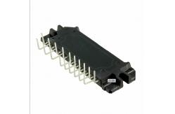
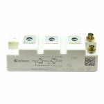
STK621-033N-E Mosfet Power Module Hybrid Inverter Circuit SIP Full Molded
|
|
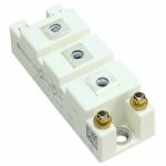
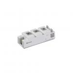
STK621-220A Mosfet Power Module Hybrid Inverter Circuit SIP Full Molded
STK621-220A INVERTER POWER HYBRID MODULE SIP Full Molded Package
Overview This IC is a 3-phase inverter power hybrid IC containing power elements (IGBT and FRD), pre-driver, overcurrent and excessive temperature protection circuit.
Application • 3-phase inverter motor drive
Features • Integrates power elements (IGBT and FRD), pre-driver, and protective circuit. • Protective circuits including overcurrent (bus line), excessive temperature and pre-drive low voltage protection are built in. • Direct input of CMOS level control signals without an insulating circuit (photocoupler, etc) is possible. • Single power supply drive is possible by using a bootstrap circuit with a built-in IC • Temperature monitor is possible by the thermistor inside the IC • Built-in simultaneous upper/lower ON prevention circuit to prevent arm shorting through simultaneous ON input for the upper and lower side transistors. (Dead time is required for preventing shorting due to switching delay.) • SIP (The single in-line package) of the transfer full mold structure.
Specifications Absolute Maximum Ratings at Tc = 25°C
In the case without the instruction, the voltage standard is - terminal = VSS terminal voltage. *1 Surge voltage developed by the switching operation due to the wiring inductance between the + and –terminals. *2 VD1 = between VB1-U, VD2 = VB2-V, VD3 = VB3-W, VB4 = VDD-VSS, terminal voltage. *3 Flatness of the heat-sink should be lower than 0.25mm. *4 The test condition is AC 2500V, 1 second.
Notes 1. Input ON voltage indicates a value to turn on output stage IGBT. Input OFF voltage indicates a value to turn off output stage IGBT. At the time of output ON, set the input signal voltage 0V to VIH (MAX). At the time of output OFF, set the input signal voltage VIL (MIN) to 5V. 2. When the internal protection circuit operates, there is a Fault signal ON (When the Fault terminal is low level, Fault signal is ON state : output form is open DRAIN) but the Fault signal doesn't latch. After protection operation ends, it returns automatically within about 18ms to 80ms and resumes operation beginning condition. So, after Fault signal detection, set OFF (HIGH) to all input signals at once. However, the operation of pre-drive power supply low voltage protection (UVLO: it has a hysteresis about 0.3V) is as follows. Upper side → There is no Fault signal output, but it does a corresponding gate signal OFF. Incidentally, it returns to the regular operation when recovering to the normal voltage, but the latch continues among input signal ON (LOW). Lower side → It outputs Fault signal with gate signal OFF. However, it is different from the protection operation of upper side, it is automatically resets about 18ms to 80ms later and resumes operation beginning condition when recovering to normal voltage. (The protection operation doesn't latch by the input signal.) 3. When assembling the hybrid IC on the heat sink with M4 type screw, tightening torque range is 0.79N•m to 1.17N•m. Flatness of the heat-sink should be lower than 0.25mm. 4. The pre-drive low voltage protection is the feature to protect a device when the pre-driver supply voltage declines with the operating malfunction. As for the pre-driver supply voltage decline in case of operation beginning, and so on, we request confirmation in the set.
|
||||||||||||||||||||||||||||||||||||||||||||||||||||||||||||||||||||||
| Product Tags: thyristor diode module hybrid inverter circuit |
|
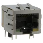
Original Connect RJ45 Ethernet Jack Plug J00-0065NL for PBC Board |
|
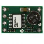
PTH04000WAH NEW AND ORIGINAL STOCK |
|
UPS161 Synchronizing signal controlling CMOS LSI tv circuit boards led driver circuit board |
|
BSM100GB60DLCHOSA1 NEW AND ORIGINAL STOCK |
|
FF150R12RT4HOSA1 NEW AND ORIGINAL STOCK |
|
FF100R12RT4HOSA1 NEW AND ORIGINAL STOCK |