
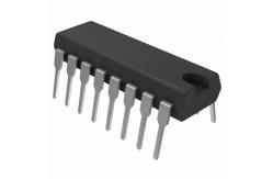
SN75173N Linear Integrated Circuits Quadruple Differential Line Receivers
|
|
SN75173 Linear Integrated Circuits Quadruple Differential Line Receivers
SN55173, SN65173, SN75173 QUADRUPLE DIFFERENTIAL LINE RECEIVERS
description The SN55173, SN65173, and SN75173 are monolithic quadruple differential line receivers with 3-state outputs. They are designed to meet the requirements of TIA/EIA-422-B, TIA/EIA-423-B, TIA/EIA-485-A, and several ITU recommendations. The standards are for balanced multipoint bus transmission at rates up to 10 megabits per second. The four receivers share two OR enable inputs, one active when high, the other active when low. These devices feature high input impedance, input hysteresis for increased noise immunity, and input sensitivity of ±200 mV over a common-mode input voltage range of –12 V to 12 V. Fail-safe design specifies that if the inputs are open circuited, the outputs are always high. The SN65173 and SN75173 are designed for optimum performance when used with the SN75172 or SN75174 quad differential line drivers. The SN55173 is characterized over the full military temperature range of –55°C to 125°C. The SN65173 is characterized for operation from –40°C to 85°C. The SN75173 is characterized for operation from 0°C to 70°C.
absolute maximum ratings over operating free-air temperature range (unless otherwise noted)† Supply voltage, VCC (see Note 1) . . . . . . . . . . . . . . . . . . . . . . . . . . . . . . . . . . . . . . . . . . . . . . . . 7 V Input voltage (VI or B inputs) . . . . . . . . . . . . . . . . . . . . . . . . . . . . . . . . . . . . . . . . . . . . . . . . . . . . ±25 V Differential input voltage, VID (see Note 2) . . . . . . . . . . . . . . . . . . . . . . . . . . . . . . . . . . . . . . . . . ±25 V Enable input voltage, VI . . . . . . . . . . . . . . . . . . . . . . . . . . . . . . . . . . . . . . . . . . . . . . . . . . . . . . . . . . 7 V Low-level output current, IOL . . . . . . . . . . . . . . . . . . . . . . . . . . . . . . . . . . . . . . . . . . . . . . . . . . . 50 mA Package thermal impedance, θJA (see Note 3): D package .. . . . . . . . . . . . . . . . . . . . . . . . . . 73 °C/W N package . . . . . . . . . . . .. . . . . . . . . . . . . . . 67 °C/W Continuous total dissipation . . . . . . . . . . . . . . . . . . . . . . . . . . . . . . . . . . . See Dissipation Rating Table Case temperature for 60 seconds, TC: FK package . . . . . . . . . . . . . . . . . . . . . . . . . . . . . . . . . . 260°C Lead temperature 1,6 mm (1/16 inch) from case for 10 seconds: D or N package . . . . . . . . . . . 260°C Lead temperature 1,6 mm (1/16 inch) from case for 60 seconds: J package . . . . . . . . . . . . . . . 300°C Storage temperature range, Tstg . . . . . . . . . . . . . . . . . . . . . . . . . . . . . . . . . . . . . . . . . –65°C to 150°C
† Stresses beyond those listed under “absolute maximum ratings” may cause permanent damage to the device. These are stress ratings only, and functional operation of the device at these or any other conditions beyond those indicated under “recommended operating conditions” is not implied. Exposure to absolute-maximum-rated conditions for extended periods may affect device reliability. NOTES: 1. All voltage values, except differential input voltage, are with respect to network ground terminal. 2. Differential input voltage is measured at the noninverting input with respect to the corresponding inverting input. 3. The package thermal impedance is calculated in accordance with JESD 51.
THE SN55173 IS NOT RECOMMENDED FOR NEW DESIGNS.
logic symbol †
logic diagram (positive logic)
schematics of inputs and outputs
|
| Product Tags: electronics ic chip integrated circuit components |

|
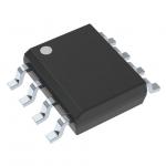
SN65HVD251DR Electronic IC Chip NEW AND ORIGINAL STOCK |
|
SN65HVD485EDR Electronic IC Chip NEW AND ORIGINAL STOCK |

|
SN65HVD11DR Electronic IC Chip NEW AND ORIGINAL STOCK |

|
SN65HVD1782DR Electronic IC Chip NEW AND ORIGINAL STOCK |

|
SN65HVD233DR Electronic IC Chip NEW AND ORIGINAL STOCK |
|
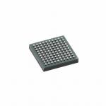
BCM54616SC0IFBG Electronic IC Chip NEW AND ORIGINAL STOCK |