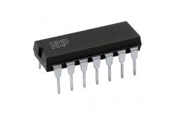
Dual JK flip-flop with reset , negative - edge trigger 74HC107N,652
|
|
FEATURES
• Output capability: standard • ICC category: flip-flop
GENERAL DESCRIPTION
The 74HC/HCT107 are high-speed Si-gate CMOS devices and are pin compatible with low power Schottky TTL (LSTTL). They are specified in compliance with JEDEC standard no. 7A.
The 74HC/HCT107 are dual negative edge triggered JK-type flip-flops featuring individual J, K, clock (nCP) and reset (nR) inputs; also complementary Q and Q outputs.
The J and K inputs must be stable one set-up time prior to the HIGH-to-LOW clock transition for predictable operation.
The reset (nR) is an asynchronous active LOW input. When LOW, it overrides the clock and data inputs, forcing the Q output LOW and the Q output HIGH.
Schmitt-trigger action in the clock input makes the circuit highly tolerant to slower clock rise and fall times.
QUICK REFERENCE DATA GND = 0 V; Tamb = 25 °C; tr = tf = 6 ns
Notes
1. CPD is used to determine the dynamic power dissipation (PD in µW): PD = CPD × VCC2 × fi + ∑ (CL × VCC2 × fo) where: fi = input frequency in MHz fo = output frequency in MHz ∑ (CL × VCC2 × fo) = sum of outputs CL = output load capacitance in pF VCC = supply voltage in V
2. For HC the condition is VI = GND to VCC For HCT the condition is VI = GND to VCC − 1.5 V.
PIN DESCRIPTION
|
|||||||||||||||||||||||||||||||||||||
| Product Tags: electronics ic chip integrated circuit components | |||||||||||||||||||||||||||||||||||||