Smart High-Side Power Switch Two Channels: 2 x 30mΩ Current Sense
Product Summary
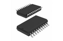
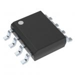
Package
| Operating Voltage
Vbb(on) |
5.0...34V | |
Active channels | one | two parallel | | On-state Resistance
RON | 30mΩ | 15mΩ | | Nominal load current
IL(NOM) | 5.5A | 8.5A | | Current limitation
IL(SCr) | 24A | 24A |
General Description
• N channel vertical power MOSFET with charge pump, ground
referenced CMOS compatible input,
diagnostic feedback and proportional load current
sense monolithically integrated in Smart SIPMOS
technology.
• Providing embedded protective functions
Applications
• µC compatible high-side power switch with diagnostic feedback for
12V and 24V grounded loads
• All types of resistive, inductive and capacitve loads
• Most suitable for loads with high inrush currents, so as lamps
• Replaces electromechanical relays, fuses and discrete circuits
Basic Functions
• CMOS compatible input
• Undervoltage and overvoltage shutdown with auto-restart and
hysteresis
• Fast demagnetization of inductive loads
• Logic ground independent from load ground
Protection Functions
• Short circuit protection
• Overload protection
• Current limitation
• Thermal shutdown
• Overvoltage protection (including load dump) with external
resistor
• Reverse battery protection with external resistor
• Loss of ground and loss of Vbb protection
• Electrostatic discharge protection (ESD)
Diagnostic Functions
• Proportinal load current sense
• Diagnostic feedback with open drain output
• Open load detection in OFF-state with external resistor
• Feedback of thermal shutdown in ON-state
Functional diagram
Maximum Ratings at Tj = 25°C unless otherwise specified | Parameter | Symbol | Values | Unit | | Supply voltage | Vbb | 43 | V | | Supply voltage for full short circuit protection Tj,start =-40 ...+150°C | Vbb | 34 | V | | Load current | IL | self-limited | A | Load dump protection1) VLoadDump = VA + Vs, VA = 13.5 V
RI 2) = 2 Ω, td = 200 ms; IN= low or high,
each channel loaded with RL = 7.0 Ω, | VLoaddump3)
| 60
| V
| Operating temperature range
Storage temperature range | Tj
Tstg | -40 ...+150
-55 ...+150 | °C
| Power dissipation (DC)4)
Ta = 25°C:
(all channels active)
Ta = 85°C: | Ptot
| | | Maximal switchable inductance, single pulse
Vbb =12V, Tj,start =150°C4),
IL = 5.5 A, EAS = 370 mJ, 0Ω
one channel:
IL = 8.5 A, EAS = 790 mJ, 0Ω
two parallel channels: |
ZL
|
18
16 |
mH | Electrostatic discharge capability (ESD)
IN:
(Human Body Model)
ST, IS:
out to all other pins
shorted:
acc. MIL-STD883D, method 3015.7 and ESD assn. std. S5.1-1993
R=1.5kΩ; C=100pF | VESD
| 1.0
4.0
8.0
| kV
| | Input voltage (DC) | VIN | -10 ... +16 | V | Current through input pin (DC)
Current through status pin (DC)
Current through current sense pin (DC) | IIN
IST
IIS | ±2.0
±5.0
±14 | mA
|
|