
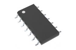
Wide Bandwidth Quad JFET Input Operational Amplifiers LF347M
|
|
LF147/LF347 Wide Bandwidth Quad JFET Input Operational Amplifiers
General Description The LF147 is a low cost, high speed quad JFET input operational amplifier with an internally trimmed input offset voltage (BI-FET II™ technology). The device requires a low supply current and yet maintains a large gain bandwidth product and a fast slew rate. In addition, well matched high voltage JFET input devices provide very low input bias and offset currents. The LF147 is pin compatible with the standard LM148. This feature allows designers to immediately upgrade the overall performance of existing LF148 and LM124 designs. The LF147 may be used in applications such as high speed integrators, fast D/A converters, sample-and-hold circuits and many other circuits requiring low input offset voltage, low input bias current, high input impedance, high slew rate and wide bandwidth. The device has low noise and offset voltage drift.
Features
Simplified Schematic Connection Diagram
DC Electrical Characteristics (Note 7)
Note 2: Absolute Maximum Ratings indicate limits beyond which damage to the device may occur. Operating Ratings indicate conditions for which the device is functional, but do not guarantee specific performance limits. Note 3: Unless otherwise specified the absolute maximum negative input voltage is equal to the negative power supply voltage. Note 4: Any of the amplifier outputs can be shorted to ground indefinitely, however, more than one should not be simultaneously shorted as the maximum junction temperature will be exceeded. Note 5: For operating at elevated temperature, these devices must be derated based on a thermal resistance of θjA. Note 6: The LF147 is available in the military temperature range −55˚C≤TA≤125˚C, while the LF347B and the LF347 are available in the commercial temperature range 0˚C≤TA≤70˚C. Junction temperature can rise to Tj max = 150˚C. Note 7: Unless otherwise specified the specifications apply over the full temperature range and for VS=±20V for the LF147 and for VS= ±15V for the LF347B/LF347. VOS, IB, and IOS are measured at VCM=0. Note 8: The input bias currents are junction leakage currents which approximately double for every 10˚C increase in the junction temperature, Tj . Due to limited production test time, the input bias currents measured are correlated to junction temperature. In normal operation the junction temperature rises above the ambient temperature as a result of internal power dissipation, PD. Tj =TA+θjA PD where θjA is the thermal resistance from junction to ambient. Use of a heat sink is recommended if input bias current is to be kept to a minimum. Note 9: Supply voltage rejection ratio is measured for both supply magnitudes increasing or decreasing simultaneously in accordance with common practice from VS = ± 5V to ±15V for the LF347 and LF347B and from VS = ±20V to ±5V for the LF147. Note 10: Refer to RETS147X for LF147D and LF147J military specifications. Note 11: Max. Power Dissipation is defined by the package characteristics. Operating the part near the Max. Power Dissipation may cause the part to operate outside guaranteed limits. Note 12: Human body model, 1.5 kΩ in series with 100 pF
|
|||||||||||||||||||||||||||||||||||||||||||||||||||||||||||||||||||||||||||||||||||||||||||||||||||||||||||||||||||||||||||||||||||||||||||||||||||||||||||||||||||||
| Product Tags: electronics ic chip integrated circuit components | |||||||||||||||||||||||||||||||||||||||||||||||||||||||||||||||||||||||||||||||||||||||||||||||||||||||||||||||||||||||||||||||||||||||||||||||||||||||||||||||||||||
|
AD8552ARUZ Electronic IC Chip NEW AND ORIGINAL STOCK |
|
BA10358F-E2 Electronic IC Chip NEW AND ORIGINAL STOCK |
|
BA14741F-E2 Electronic IC Chip NEW AND ORIGINAL STOCK |
|
DRV602PWR Flash Memory IC NEW AND ORIGINAL STOCK |
|
OPA335AIDR Electronic IC Chips SINGLE-SUPPLY CMOS OPERATIONAL AMPLIFIERS |
|
OP90GSZ-REEL7 Electronic IC Chips Low-Voltage Operational Amplifier |