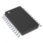
CD4051BPWR Integrated Circuit Chip CMOS Analog Multiplexers/Demultiplexers with Logic Level Conversion
|
CMOS Analog Multiplexers/Demultiplexers with Logic Level ConversionThe CD4051B, CD4052B, and CD4053B analog multiplexers are digitally-controlled analog switches having low ON impedance and very low OFF leakage current. Control of analog signals up to 20VP-P can be achieved by digital signal amplitudes of 4.5V to 20V (if VDD-VSS = 3V, a VDD-VEE of up to 13V can be controlled; for VDD-VEE level differences above 13V, a VDD-VSS of at least 4.5V is required).
For example, if VDD = +4.5V, VSS = 0V, and VEE = -13.5V, analog signals from -13.5V to +4.5V can be controlled by digital inputs of 0V to 5V. These multiplexer circuits dissipate extremely low quiescent power over the full VDD-VSS and VDD-VEE supply-voltage ranges, independent of the logic state of the control signals. When a logic “1” is present at the inhibit input terminal, all channels are off.
Features • Wide Range of Digital and Analog Signal Levels - Digital . . . . . . . . . . . . . . . . . . . . . . . . . . . . . . 3V to 20V - Analog. . . . . . . . . . . . . . . . . . . . . . . . . . . . . . . ≤20VP-P • Low ON Resistance, 125Ω (Typ) Over 15VP-P Signal Input Range for VDD-VEE = 18V • High OFF Resistance, Channel Leakage of ±100pA (Typ) at VDD-VEE = 18V • Logic-Level Conversion for Digital Addressing Signals of 3V to 20V (VDD-VSS = 3V to 20V) to Switch Analog Signals to 20VP-P (VDD-VEE = 20V) • Matched Switch Characteristics, rON = 5Ω (Typ) for VDD-VEE = 15V • Very Low Quiescent Power Dissipation Under All DigitalControl Input and Supply Conditions, 0.2µW (Typ) at VDD-VSS = VDD-VEE = 10V
Typical Performance Curves
Functional Block Diagrams
|
| Product Tags: integrated circuit ic integrated circuit components |