
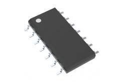
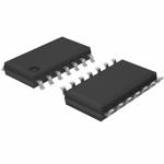
Low Power Consumption Integrated Circuit Chip Jfet-Input Operational Amplifiers TL084IDR
|
|
JFET-INPUT OPERATIONAL AMPLIFIERS TL084IDR
*Low Power Consumption *Wide Common-Mode and Differential Voltage Ranges *Low Input Bias and Offset Currents *Output Short-Circuit Protection *Low Total Harmonic Distortion . . . 0.003% Typ *High Input Impedance . . . JFET-Input Stage *Latch-Up-Free Operation *High Slew Rate . . . 13 V/µs Typ *Common-Mode Input Voltage Range Includes VCC+
Description The TL08x JFET-input operational amplifier family is designed to offer a wider selection than any previously developed operational amplifier family. Each of these JFET-input operational amplifiers incorporates well-matched, high-voltage JFET and bipolar transistors in a monolithic integrated circuit. The devices feature high slew rates, low input bias and offset currents, and low offset-voltage temperature coefficient. Offset adjustment and external compensation options are available within the TL08x family.
The C-suffix devices are characterized for operation from 0°C to 70°C. The I-suffix devices are characterized for operation from −40°C to 85°C. The Q-suffix devices are characterized for operation from −40°C to 125°C. The M-suffix devices are characterized for operation over the full military temperature range of −55°C to 125°C.
schematic (each amplifier)
absolute maximum ratings over operating free-air temperature range (unless otherwise noted)†
†Stresses beyond those listed under “absolute maximum ratings” may cause permanent damage to the device. These are stress ratings only, and functional operation of the device at these or any other conditions beyond those indicated under “recommended operating conditions” is not implied. Exposure to absolute-maximum-rated conditions for extended periods may affect device reliability. NOTES: 1. All voltage values, except differential voltages, are with respect to the midpoint between VCC+ and VCC−. 2. Differential voltages are at IN+ with respect to IN−. 3. The magnitude of the input voltage must never exceed the magnitude of the supply voltage or 15 V, whichever is less. 4. The output may be shorted to ground or to either supply. Temperature and/or supply voltages must be limited to ensure that the dissipation rating is not exceeded. 5. Maximum power dissipation is a function of TJ(max), θJA, and TA. The maximum allowable power dissipation at any allowable ambient temperature is PD = (TJ(max) − TA)/θJA. Operating at the absolute maximum TJ of 150°C can affect reliability. 6. The package thermal impedance is calculated in accordance with JESD 51-7.
DISSIPATION RATING TABLE
|
|||||||||||||||||||||||||||||||||||||||||||||||||||||||||||||||||||||||||||||||||||||||||||||||||||||||||||||||||||||||||||||||||||||||||||||||||||||||||||||||||
| Product Tags: integrated circuit ic integrated circuit components | |||||||||||||||||||||||||||||||||||||||||||||||||||||||||||||||||||||||||||||||||||||||||||||||||||||||||||||||||||||||||||||||||||||||||||||||||||||||||||||||||
|
AD8552ARUZ Electronic IC Chip NEW AND ORIGINAL STOCK |
|
BA10358F-E2 Electronic IC Chip NEW AND ORIGINAL STOCK |
|
BA14741F-E2 Electronic IC Chip NEW AND ORIGINAL STOCK |
|
DRV602PWR Flash Memory IC NEW AND ORIGINAL STOCK |
|
OPA335AIDR Electronic IC Chips SINGLE-SUPPLY CMOS OPERATIONAL AMPLIFIERS |
|
OP90GSZ-REEL7 Electronic IC Chips Low-Voltage Operational Amplifier |