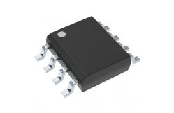
Lincmose Programmable Low Power Operational Amplifiers TLC271CDR
|
|
LinCMOSTM PROGRAMMABLE LOW-POWER OPERATIONAL AMPLIFIERS
*Input Offset Voltage Drift ...Typically 0.1 µV/Month, Including the First 30 Days *Wide Range of Supply Voltages Over Specified Temperature Range: 0°C to 70°C . . . 3 V to 16 V –40°C to 85°C . . . 4 V to 16 V –55°C to 125°C . . . 5 V to 16 V *Single-Supply Operation *Common-Mode Input Voltage Range Extends Below the Negative Rail (C-Suffix and I-Suffix Types) *Low Noise . . . 25 nV/√Hz Typically at f = 1 kHz (High-Bias Mode) *Output Voltage Range Includes Negative Rail *High Input Impedance . . . 1012 Ω Typ *ESD-Protection Circuitry *Small-Outline Package Option Also Available in Tape and Reel *Designed-In Latch-Up Immunity
description The TLC271 operational amplifier combines a wide range of input offset voltage grades with low offset voltage drift and high input impedance. In addition, the TLC271 offers a bias-select mode that allows the user to select the best combination of power dissipation and ac performance for a particular application. These devices use Texas Instruments silicon-gate LinCMOSTM technology, which provides offset voltage stability far exceeding the stability available with conventional metal-gate processes.
DEVICE FEATURES
†Typical at VDD = 5 V, TA = 25°C
equivalent schematic
absolute maximum ratings over operating free-air temperature (unless otherwise noted)† Supply voltage, VDD (see Note 1) . . . . . . . . . . . . . . . . . . . . . . . . . . . . . . . . . . . . . . . . . . . . . . . . . . . 18 V Differential input voltage, VID (see Note 2) . . . . . . . . . . . . . . . . . . . . . . . . . . . . . . . . . . . . . . . . .. . . ±VDD Input voltage range, VI (any input) . . . . . . . . . . . . . . . . . . . . . . . . . . . . . . . . . . . . . . . . . . . – 0.3 V to VDD Input current, II . . . . . . . . . . . . . . . . . . . . . . . . . . . . . . . . . . . . . . . . . . . . . . . . . . . . . . . . . . . . . . . . . ±5 mA Output current, IO . . . . . . . . . . . . . . . . . . . . . . . . . . . . . . . . . . . . . . . . . . . . . . . . . . . . . . . . . . . . . . ±30 mA Duration of short-circuit current at (or below) 25°C (see Note 3) . . . . .. . . . . . . . . . . . . . . . . . . . .Unlimited Continuous total dissipation . . . . . . . . . . . . . . . . . . . . . . . . . . . . . . . . . . . . . See Dissipation Rating Table Operating free-air temperature, TA: C suffix . . . . . . . . . . . . . . . . . . . . . . . . . . . . . . . . . . . . . .0 °C to 70°C I suffix . . . . . . . . . . . . . . . . . . . . . . . . . . . . . . . . . . . . – 40°C to 85°C M suffix . . . . . . . . . . . . . . . . . . . . . . . . . . . . . . . . . . . – 55°C to 125°C Storage temperature range . . . . . . . . . . . . . . . . . . . . . . . . . . . . . . . . . . . . . . . . . . . . . . . – 65°C to 150°C Case temperature for 60 seconds: FK package . . . . . . . . . . . . . . . . . . . . . . . . . . . . . . . . . . . . . . . 260°C Lead temperature 1,6 mm (1/16 inch) from case for 10 seconds: D or P package . . . . . . . . . . . . . .260°C Lead temperature 1,6 mm (1/16 inch) from case for 60 seconds: JG package . . . . . . . . . . . . . . . . .300°C
† Stresses beyond those listed under “absolute maximum ratings” may cause permanent damage to the device. These are stress ratings only, and functional operation of the device at these or any other conditions beyond those indicated under “recommended operating conditions” is not implied. Exposure to absolute-maximum-rated conditions for extended periods may affect device reliability. NOTES: 1. All voltage values, except differential voltages, are with respect to network ground. 2. Differential voltages are at IN+ with respect to IN–. 3. The output may be shorted to either supply. Temperature and/or supply voltages must be limited to ensure that the maximum dissipation rating is not exceeded (see application section).
DISSIPATION RATING TABLE
recommended operating conditions
|
||||||||||||||||||||||||||||||||||||||||||||||||||||||||||||||||||||||||||||||||||||||||||||||
| Product Tags: electronics ic chip integrated circuit components | ||||||||||||||||||||||||||||||||||||||||||||||||||||||||||||||||||||||||||||||||||||||||||||||
|
AD8552ARUZ Electronic IC Chip NEW AND ORIGINAL STOCK |
|
BA10358F-E2 Electronic IC Chip NEW AND ORIGINAL STOCK |
|
BA14741F-E2 Electronic IC Chip NEW AND ORIGINAL STOCK |
|
DRV602PWR Flash Memory IC NEW AND ORIGINAL STOCK |
|
OPA335AIDR Electronic IC Chips SINGLE-SUPPLY CMOS OPERATIONAL AMPLIFIERS |
|
OP90GSZ-REEL7 Electronic IC Chips Low-Voltage Operational Amplifier |

