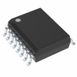
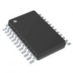
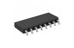
8 Channel Integrated Circuit Chip Analog Multiplexer / Demultiplexer 74HC4051D
|
|
1. General description
The 74HC4051; 74HCT4051 is a high-speed Si-gate CMOS device and is pin compatible with Low-power Schottky TTL (LSTTL). The device is specified in compliance with JEDEC standard no. 7A.
The 74HC4051; 74HCT4051 is an 8-channel analog multiplexer/demultiplexer with three digital select inputs (S0 to S2), an active-LOW enable input (E), eight independent inputs/outputs (Y0 to Y7) and a common input/output (Z). With E LOW, one of the eight switches is selected (low impedance ON-state) by S0 to S2.
With E HIGH, all switches are in the high-impedance OFF-state, independent of S0 to S2. VCC and GND are the supply voltage pins for the digital control inputs (S0 to S2, and E). The VCC to GND ranges are 2.0 V to 10.0 V for 74HC4051 and 4.5 V to 5.5 V for 74HCT4051. The analog inputs/outputs (Y0 to Y7, and Z) can swing between VCC as a positive limit and VEE as a negative limit. VCC VEE may not exceed 10.0 V.
For operation as a digital multiplexer/demultiplexer, VEE is connected to GND (typically ground).
2. Features and benefits
Wide analog input voltage range from -5 V to +5 V Low ON resistance: 80 Ω (typical) at VCC - VEE = 4.5 V 70 Ω (typical) at VCC - VEE = 6.0 V 60 Ω (typical) at VCC - VEE = 9.0 V Logic level translation: to enable 5 V logic to communicate with +-5 V analog signals Typical ‘break before make’ built-in ESD protection: HBM JESD22-A114F exceeds 2000 V MM JESD22-A115-A exceeds 200 V Multiple package options Specified from -40 ℃ to +85 ℃ and -40 ℃ to +125℃
3. Applications
Analog multiplexing and demultiplexing Digital multiplexing and demultiplexing Signal gating
4. Ordering information
5. Functional diagram
|
||||||||||||||||||||||||||||||||||
| Product Tags: integrated circuit ic integrated circuit components | ||||||||||||||||||||||||||||||||||