
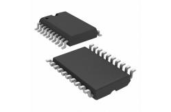
SN74HC541DWR Integrated Circuit Chip linear digital integrated circuit
|
|
Stock Offer (Hot Sell)
SN54HC541, SN74HC541 OCTAL BUFFERS AND LINE DRIVERS WITH 3-STATE OUTPUTS
* Wide Operating Voltage Range of 2 V to 6 V * High-Current 3-State Outputs Drive Bus Lines Directly or Up To 15 LSTTL Loads * Low Power Consumption, 80-µA Max ICC * Typical tpd = 10 ns * ±6-mA Output Drive at 5 V * Low Input Current of 1 µA Max * Data Flow-Through Pinout (All Inputs on Opposite Side From Outputs)
description These octal buffers and line drivers feature the performance of the ’HC240 devices and a pinout with inputs and outputs on opposite sides of the package. This arrangement greatly facilitates printed circuit board layout.
The 3-state outputs are controlled by a two-input NOR gate. If either output-enable (OE1 or OE2) input is high, all eight outputs are in the high-impedance state. The ’HC541 devices provide true data at the outputs.
absolute maximum ratings over operating free-air temperature range (unless otherwise noted)†
Supply voltage range, VCC . . . . . . . . . . . . . . . . . . . . . . . . . . . . . . . . . . . . . . . . . . . . . . –0.5 V to 7 V Input clamp current, IIK (VI < 0 or VI > VCC) (see Note 1) . . . . . . . . . . . . . . . . . . . . . . . . . . . . ±20 mA Output clamp current, IOK (VO < 0 or VO > VCC) (see Note 1) . . . . . . . . . . . . . . . . . . . . . . . . ±20 mA Continuous output current, IO (VO = 0 to VCC) . . . . . . . . . . . . . . . . . . . . . . . . . . . . . . . . . . . . ±35 mA Continuous current through VCC or GND . . . . . . . . . . . . . . . . . . . . . . . . . . . . . . . . . . . . . . . . ±70 mA Package thermal impedance, θJA (see Note 2): DB package . . . . . . . . . . . . . . . . . . . . . . . . . 70°C/W DW package . . . . . . . . . . . . . . . . . . . . . . . . . 58°C/W N package . . . . . . . . . . . . . . . . . . . . . . . . . . . 69°C/W NS package . . . . . . . . . . . . . . . . . . . . . . . . . . 60°C/W PW package . . . . . . . . . . . . . . . . . . . . . . . . . . 83°C/W Storage temperature range, Tstg . . . . . . . . . . . . . . . . . . . . . . . . . . . . . . . . . . . . . . . . . –65°C to 150°C
†Stresses beyond those listed under “absolute maximum ratings” may cause permanent damage to the device. These are stress ratings only, and functional operation of the device at these or any other conditions beyond those indicated under “recommended operating conditions” is not implied. Exposure to absolute-maximum-rated conditions for extended periods may affect device reliability. NOTES: 1. The input and output voltage ratings may be exceeded if the input and output current ratings are observed. 2. The package thermal impedance is calculated in accordance with JESD 51-7.
logic diagram (positive logic)
|
|||||||||||||||||||||||||||||||||||||||||||||||||||||||||||||||||||||||||||||||||||||||||||||||||||||||||||||||||||||||||||||||||||||||||||||||||||||||||||
| Product Tags: electronics ic chip integrated circuit ic |

|
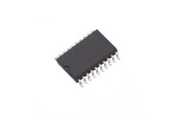
SN65HVD251DR Electronic IC Chip NEW AND ORIGINAL STOCK |
|
SN65HVD485EDR Electronic IC Chip NEW AND ORIGINAL STOCK |

|
SN65HVD11DR Electronic IC Chip NEW AND ORIGINAL STOCK |

|
SN65HVD1782DR Electronic IC Chip NEW AND ORIGINAL STOCK |

|
SN65HVD233DR Electronic IC Chip NEW AND ORIGINAL STOCK |
|
BCM54616SC0IFBG Electronic IC Chip NEW AND ORIGINAL STOCK |