
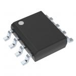
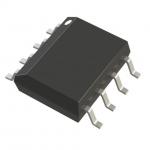
LM6172IMX Integrated Circuit Chip amplifier ic chip
|
|
Stock Offer (Hot Sell)
LM6172 Dual High Speed, Low Power, Low Distortion, Voltage Feedback Amplifiers
General Description The LM6172 is a dual high speed voltage feedback amplifier. It is unity-gain stable and provides excellent DC and AC performance. With 100 MHz unity-gain bandwidth, 3000V/µs slew rate and 50 mA of output current per channel, the LM6172 offers high performance in dual amplifiers; yet it only consumes 2.3 mA of supply current each channel.
The LM6172 operates on ±15V power supply for systems requiring large voltage swings, such as ADSL, scanners and ultrasound equipment. It is also specified at ±5V power supply for low voltage applications such as portable video systems.
The LM6172 is built with National’s advanced VIP™ III (Vertically Integrated PNP) complementary bipolar process. See the LM6171 datasheet for a single amplifier with these same features.
Features (Typical Unless Otherwise Noted)
Applications
Absolute Maximum Ratings (Note 1) If Military/Aerospace specified devices are required, please contact the National Semiconductor Sales Office/ Distributors for availability and specifications.
ESD Tolerance (Note 2) Human Body Model 3 kV Machine Model 300V Supply Voltage (V+ − V− ) 36V Differential Input Voltage (Note 5) ±10V Output Short Circuit to Ground (Note 3) Continuous Storage Temp. Range −65˚C to +150˚C Maximum Junction Temperature (Note 4) 150˚C
Operating Ratings(Note 1) Supply Voltage 5.5V ≤ VS ≤ 36V Junction Temperature Range LM6172I −40˚C ≤ TJ ≤ +85˚C Thermal Resistance (θJA) N Package, 8-Pin Molded DIP 95˚C/W M Package, 8-Pin Surface Mount 160˚C/W
Note 1: Absolute Maximum Ratings indicate limits beyond which damage to the device may occur. Operating Ratings indicate conditions for which the device is intended to be functional, but specific performance is not guaranteed. For guaranteed specifications and the test conditions, see the Electrical Characteristics. Note 2: Human body model, 1.5 kΩ in series with 100 pF. Machine Model, 200Ω in series with 100 pF. Note 3: Continuous short circuit operation can result in exceeding the maximum allowed junction temperature of 150˚C. Note 4: The maximum power dissipation is a function of TJ(max), θJA, and TA. The maximum allowable power dissipation at any ambient temperature is PD = (TJ(max) − TA)/θJA. All numbers apply for packages soldered directly into a PC board. Note 5: Differential gain and phase are measured with AV = +2, VIN = 1 VPP at 3.58 MHz and both input and output 75Ω terminated.
LM6172 Driving Capacitive Load
Connection Diagram
|
|||||||||||||||||||||||||||||||||||||||||||||||||||||||||||||||||||||||||||||||||||||||||||||||||||||||||||||||||||||||||||||||||||||||||||||||||||||||||||
| Product Tags: electronics ic chip integrated circuit components |
|
AD8552ARUZ Electronic IC Chip NEW AND ORIGINAL STOCK |
|
BA10358F-E2 Electronic IC Chip NEW AND ORIGINAL STOCK |
|
BA14741F-E2 Electronic IC Chip NEW AND ORIGINAL STOCK |
|
DRV602PWR Flash Memory IC NEW AND ORIGINAL STOCK |
|
OPA335AIDR Electronic IC Chips SINGLE-SUPPLY CMOS OPERATIONAL AMPLIFIERS |
|
OP90GSZ-REEL7 Electronic IC Chips Low-Voltage Operational Amplifier |