
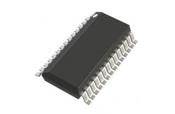
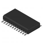
LTC3707EGN#PBF High Effi ciency,2-Phase Synchronous Step-Down Switching Regulator
|
|
LTC3707EGN High Effi ciency,2-Phase Synchronous Step-Down Switching Regulator
FEATURES
180° Phased Dual Controllers Reduce Required Input Capacitance and Power Supply Induced Noise OPTI-LOOP® Compensation Minimizes COUT ±1.5% Output Voltage Accuracy over Temperature Dual N-Channel MOSFET Synchronous Drive Power Good Output Voltage Monitor DC Programmed Fixed Frequency 150kHz to 300kHz Wide VIN Range: 4.5V to 28V Operation Very Low Dropout Operation: 99% Duty Cycle Adjustable Soft-Start Current Ramping Foldback Output Current Limiting Latched Short-Circuit Shutdown with Defeat Option Output Overvoltage Protection Remote Output Voltage Sense Low Shutdown IQ: 20μA 5V and 3.3V Standby Regulators Selectable Constant Frequency, Burst Mode® Operation or PWM Operation Small 28-Lead Narrow SSOP Package
APPLICATIONS
Notebook and Palmtop Computers, PDAs Battery Chargers Portable Instruments Battery-Operated Digital Devices DC Power Distribution Systems
DESCRIPTION
The LTC®3707 is a high performance dual step-down switching regulator controller that drives N-channel synchronous power MOSFET stages. A constant frequency current mode architecture allows adjustment of the frequency up to 300kHz. Power loss and noise due to the ESR of the input capacitors are minimized by operating the two controller output stages out of phase.
OPTI-LOOP compensation allows the transient response to be optimized over a wide range of output capacitance and ESR values. The precision 0.8V reference and power good output indicator are compatible with future microprocessor generations, and a wide 3.5V to 30V input supply range encompasses all battery chemistries.
A RUN/SS pin for each controller provides both soft-start and optional timed, short-circuit shutdown. Current foldback limits MOSFET dissipation during short-circuit conditions when overcurrent latchoff is disabled. Output overvoltage protection circuitry latches on the bottom MOSFET until VOUT returns to normal. The FCB mode pin can select among Burst Mode operation, constant frequency mode and continuous inductor current mode or regulate a secondary winding.
ABSOLUTE MAXIMUM RATINGS
Input Supply Voltage (VIN) .........................30V to –0.3V Top Side Driver Voltages (BOOST1, BOOST2) ................................... 36V to –0.3V Switch Voltage (SW1, SW2) ......................... 30V to –5V INTVCC, EXTVCC, RUN/SS1, RUN/SS2, (BOOST1-SW1), (BOOST2-SW2), PGOOD .............................. 7V to –0.3V SENSE1+, SENSE2+, SENSE1–, SENSE2– Voltages .........................(1.1)INTVCC to –0.3V FREQSET, STBYMD, FCB Voltage ......... INTVCC to –0.3V ITH1, ITH2, VOSENSE1, VO SENSE2 Voltages ... 2.7V to –0.3V Peak Output Current <10μs (TG1, TG2, BG1, BG2) .....3A INTVCC Peak Output Current ................................. 40mA Operating Temperature Range (Note 2).... –40°C to 85°C Junction Temperature (Note 3) ............................. 125°C Storage Temperature Range ................... –65°C to 150°C Lead Temperature (Soldering, 10 sec) .................. 300°C
Hot selling offer!!!
|
|
BTS724GXUMA1 Smart High-Side Power Switch Four Channels programmed integrated led circuit board |
|
TPS61041DBVR Electronic IC Chips LOW-POWER DC/DC BOOST CONVERTER |
|
US90AEVK Electronic IC Chips power ic chip 24V Hall IC Fan Driver |
|
TLE4226G Integrated Circuit Chip Intelligent Sixfold Low-Side Switch |
|
NCP1234AD65R2G Fixed Frequency Current Mode Controller for Flyback Converters |
|
REG1117FA-5.0 Integrated Circuit IC Chip Low Dropout Positive Regulator |