
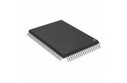
CY7C1372D-167AXI Integrated Circuit Chip 18-Mbit Pipelined SRAM
|
|
CY7C1370D CY7C1372D 18-Mbit (512K x 36/1M x 18) Pipelined SRAM with NoBL™ Architecture
Features • Pin-compatible and functionally equivalent to ZBT™ • Supports 250-MHz bus operations with zero wait states — Available speed grades are 250, 225, 200, and 167 MHz • Internally self-timed output buffer control to eliminate the need to use asynchronous OE • Fully registered (inputs and outputs) for pipelined operation • Byte Write capability
• Single 3.3V power supply • 3.3V/2.5V I/O power supply • Fast clock-to-output times — 2.6 ns (for 250-MHz device) — 2.8 ns (for 225-MHz device) — 3.0 ns (for 200-MHz device) — 3.4 ns (for 167-MHz device)
• Clock Enable (CEN) pin to suspend operation • Synchronous self-timed writes • Available in lead-Free 100 TQFP, 119 BGA, and 165 fBGA packages • IEEE 1149.1 JTAG Boundary Scan • Burst capability—linear or interleaved burst order • “ZZ” Sleep Mode option and Stop Clock option
Functional Description The CY7C1370D and CY7C1372D are 3.3V, 512K x 36 and 1 Mbit x 18 Synchronous pipelined burst SRAMs with No Bus Latency™ (NoBL™) logic, respectively. They are designed to support unlimited true back-to-back Read/Write operations with no wait states. The CY7C1370D and CY7C1372D are equipped with the advanced (NoBL) logic required to enable consecutive Read/Write operations with data being transferred on every clock cycle. This feature dramatically improves the throughput of data in systems that require frequent Write/Read transitions. The CY7C1370D and CY7C1372D are pin compatible and functionally equivalent to ZBT devices.
All synchronous inputs pass through input registers controlled by the rising edge of the clock. All data outputs pass through output registers controlled by the rising edge of the clock. The clock input is qualified by the Clock Enable (CEN) signal, which when deasserted suspends operation and extends the previous clock cycle.
Write operations are controlled by the Byte Write Selects (BWa–BWd for CY7C1370D and BWa–BWb for CY7C1372D) and a Write Enable (WE) input. All writes are conducted with on-chip synchronous self-timed write circuitry.
Three synchronous Chip Enables (CE1, CE2, CE3) and an asynchronous Output Enable (OE) provide for easy bank selection and output three-state control. In order to avoid bus contention, the output drivers are synchronously three-stated during the data portion of a write sequence.
Logic Block Diagram-CY7C1370D (512K x 36)
Logic Block Diagram-CY7C1372D (1 Mbit x 18)
Maximum Ratings (Above which the useful life may be impaired. For user guidelines, not tested.) Storage Temperature ......................................................................–65°C to +150°C Ambient Temperature with Power Applied.........................................–55°C to +125°C Supply Voltage on VDD Relative to GND............................................ –0.5V to +4.6V DC to Outputs in Tri-State ..................................................... –0.5V to VDDQ + 0.5V DC Input Voltage........................................................................–0.5V to VDD + 0.5V Current into Outputs (LOW)............................................................................ 20 mA Static Discharge Voltage.............................................................................. > 2001V (per MIL-STD-883, Method 3015) Latch-up Current........................................................................................ > 200 mA
Stock Offer (Hot Sell)
|
|||||||||||||||||||||||||||||||||||||||||||||||||||||||||||||||||||||||||||||||||||||||||||||||||||||||||||||||||||||||||||||||||||||||||||||||||||||||||||
| Product Tags: electronics ic chip integrated circuit components |
|
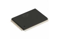
SST26VF032B-104I/MF FLASH Memory IC 32Mbit SPI - Quad I/O 104 MHz 8-WDFN (5x6) |

|
SST26VF032B-104I/MF Flash Memory Chip IC Micro 32 Mbit Low Power Consumption |
|
LPC1768FBD100K MCU Chips IC MCU 32BIT 512KB FLASH 100LQFP 32 BIT Micro Controllers |

|
EPCS16SI8N NEW AND ORIGINAL STOCK |
|
Professional Flash Memory Products Ic Memory Chip XCF08PVOG48C |

|
M45PE10-VMN6P Flash Memory IC NEW AND ORIGINAL STOCK |