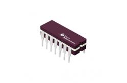
SN7406N Hex Inverter Buffers / Drivers Integrated Circuit Chip With Open Collector
|
|
SN7406N
Supply voltage, VCC (see Note 1). . . . . . . . . . . . . . . . . . . . . . . . . . . . . . . . . . . . . . . . . . . 7 V Input voltage, VI (see Note 1) . . . . . . . . . . . . . . . . . . . . . . . . . . . . . . . . . . . . . . . . . . . . . . 5.5 V Output voltage, VO (see Notes 1 and 2): SN5406, SN7406 . . . . . .
. . . . . . . . . . . . . . . . . 30 V N package 80 . . . . . . . . . . . . . . . . . . . . . 80°C/W
NS package 76 . . . . . . . . . . . . . . . . . . .
. 76°C/W † Stresses beyond those listed under “absolute maximum ratings” may cause permanent damage to the device. These are stress ratings only, and functional operation of the device at these or any other conditions beyond those indicated under “recommended operating conditions” is not implied. Exposure to absolute-maximum-rated conditions for extended periods may affect device reliability. NOTES: 1. Voltage values are with respect to network ground terminal 2. This is the maximum voltage which should be applied to any output when it is in the off state 3. The
package thermal impedance is calculated in accordance with JESD
51-7.
Stock Offer (Hot Sell)
|
|||||||||||||||||||||||||||||||||||||||||||||||||||||||||||||||||||||||||||||||||||||||||||||||||||||||||||||||||||||||||||||||||||||||||||||||||||||||||||
| Product Tags: electronics ic chip integrated circuit ic |