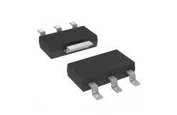
LM317DCYR 3-TERMINAL ADJUSTABLE REGULATOR
FEATURES
Output Voltage Range Adjustable From 1.25 V
Thermal Overload Protection to 37 V
Output Safe-Area Compensation
Output Current Greater Than 1.5 A
Internal Short-Circuit Current Limiting
DESCRIPTION/ORDERING INFORMATION
LM317 3-TERMINAL ADJUSTABLE REGULATOR SLVS044R–SEPTEMBER
1997–REVISED APRIL 2007 • Output Voltage Range Adjustable From 1.25
V • Thermal Overload Protection to 37 V • Output Safe-Area
Compensation • Output Current Greater Than 1.5 A • Internal
Short-Circuit Current Limiting The LM317 is an adjustable
three-terminal positive-voltage regulator capable of supplying more
than 1.5 A over an output-voltage range of 1.25 V to 37 V. It is
exceptionally easy to use and requires only two external resistors
to set the output voltage. Furthermore, both line and load
regulation are better than standard fixed regulators.
In addition to having higher performance than fixed regulators,
this device includes on-chip current limiting, thermal overload
protection, and safe operating-area protection. All overload
protection remains fully functional, even if the ADJUST terminal is
disconnected.
The LM317 is versatile in its applications, including uses in
programmable output regulation and local on-card regulation. Or, by
connecting a fixed resistor between the ADJUST and OUTPUT
terminals, the LM317 can function as a precision current regulator.
An optional output capacitor can be added to improve transient
response. The ADJUST terminal can be bypassed t
ORDERING INFORMATION(1)
| TA | PACKAGE(2) | ORDERABLE PART NUMBER | TOP-SIDE MARKING |
| 0°C to 125°C | PowerFLEX™ – KTE | Reel of 2000 | LM317KTER | LM317 |
| SOT-223 – DCY | Tube of 80 | LM317DCY | L3 |
| Reel of 2500 | LM317DCYR |
| TO-220– KC | Tube of 50 | LM317KC | LM317 |
| TO-220, short shoulder – KCS | Tube of 20 | LM317KCS |
| TO-263 – KTT | Reel of 500 | LM317KTTR | LM317 |
Absolute Maximum Ratings (1)
over virtual junction temperature range (unless otherwise noted)
| | MIN MAX | UNIT |
| VI – VO Input-to-output differential voltage | 40 | V |
| TJ Operating virtual junction temperature | 150 | °C |
| Lead temperature 1,6 mm (1/16 in) from case for 10 s | 260 | °C |
| Tstg Storage temperature range | 150 | °C |
(1) Stresses beyond those listed under "absolute maximum ratings"
may cause permanent damage to the device. These are stress ratings
only, and functional operation of the device at these or any other
conditions beyond those indicated under "recommended operating
conditions" is not implied. Exposure to absolute-maximum-rated
conditions for extended periods may affect device reliability.
Package Thermal Data (1)
| PACKAGE | BOARD | θJA | θJC | θJP (2) |
| PowerFLEX™ (KTE) | High K, JESD 51-5 | 23°C/W | 3°C/W | |
| SOT-223 (DCY) | High K, JESD 51-7 | 53°C/W | 30.6°C/W | |
| TO-220 (KC/KCS) | High K, JESD 51-5 | 19°C/W | 17°C/W | 3°C/W |
| TO-263 (KTT) | High K, JESD 51-5 | 25.3°C/W | 18°C/W | 1.94°C/W |
(1) Maximum power dissipation is a function of TJ(max), θJA, and
TA. The maximum allowable power dissipation at any allowable
ambient temperature is PD = (TJ(max) – TA)/θJA. Operating at the
absolute maximum TJ of 150°C can affect reliability.
(2) For packages with exposed thermal pads, such as QFN, PowerPAD™,
or PowerFLEX™, θJP is defined as the thermal resistance between the
die junction and the bottom of the exposed pad
Recommended Operating Conditions
| | MIN MAX | UNIT |
| VO Input-to-output differential voltage | 3 40 | V |
| IO Output current | 1.5 | A |
| TJ Operating virtual junction temperature | 0 125 | °C |
Electrical Characteristics
over recommended ranges of operating virtual junction temperature
(unless otherwise noted)
| PARAMETER | TEST CONDITIONS(1) | MIN TYP MAX | UNIT |
| Line regulation(2) | VI – VO = 3 V to 40 V | | TJ = 25°C | 0.01 0.04 | %/V |
| TJ = 0°C to 125°C | 0.02 0.07 |
| Load regulation | O = 10 mA to 1500 mA | TJ = 25°C | VO ≤ 5 V |
25 | mV |
| VO ≥ 5 V | 0.1
0.5 | %VO |
| TJ = 0°C to 125°C | VO ≤ 5 V | 20
70 | mV |
| VO ≥ 5 V | 0.3
1.5 | %VO |
| Thermal regulation | 20-ms pulse, TJ = 25°C | | | 0.03
0.07 | %VO/W |
| ADJUST terminal current | | | | 50
100 | µA |
Change in ADJUST terminal current | VI – VO = 2.5 V to 40 V, PD ≤ 20 W, IO = 10 mA to 1500 mA | | | 0.2
5 | µA |
| Reference voltage | VI – VO = 3 V to 40 V, PD ≤ 20 W, IO = 10 mA to 1500 mA | | | 1.2 1.25 1.3 | V |
Output-voltage temperature stability | TJ = 0°C to 125°C | | | 0.7 | %VO |
Minimum load current to maintain regulation | VI – VO = 40 V | | | 3.5
10 | mA |
| Maximum output current | VI – VO ≤ 15 V, PD < PMAX (4) | | | 1.5 2.2 | A |
| VI – VO ≤ 40 V, PD < PMAX (4) , TJ = 25°C | | | 0.15 0.4 |
| RMS output noise voltage(% of VO) | = 10 Hz to 10 kHz, TJ = 25°C | | | 0.003 | %VO |
| Ripple rejection | VO = 10 V, f = 120 Hz | | CADJ = 0 µF(3) | 57 | dB |
| | CADJ = 10 µF(3) | 62 64 |
| Long-term stability | TJ = 25°C | | | 0.3
1 | %/1k hr |
(1) Unless otherwise noted, the following test conditions apply:
|VI – VO| = 5 V and IOMAX = 1.5 A, TJ = 0°C to 125°C. Pulse testing
techniques are used to maintain the junction temperature as close
to the ambient temperature as possible. (2) Line regulation is
expressed here as the percentage change in output voltage per 1-V
change at the input. (3) CADJ is connected between the ADJUST
terminal and GND. (4) Maximum power dissipation is a function of
TJ(max), θJA, and TA. The maximum allowable power dissipation at
any allowable ambient temperature is PD = (TJ(max) – TA)/θJA.
Operating at the absolute maximum TJ of 150°C can affect
reliability.
Hot selling offer!!!
| Part Number | Qty | D/C | Package |
| LTC1574CS-3.3#TRPBF | 12500 | 17+ | SOIC |
| LTC1574CS-5#PBF | 12500 | 17+ | SOIC |
| LTC1574CS-5#TRPBF | 12500 | 17+ | SOIC |
| LTC1588CG#PBF | 12500 | 17+ | SSOP |
| LTC1588CG#TRPBF | 12500 | 17+ | SSOP |
| LTC1588IG#PBF | 12500 | 17+ | SSOP |
| LTC1588IG#TRPBF | 12500 | 17+ | SSOP |
| LTC1589CG#PBF | 12500 | 17+ | SSOP |
| LTC1589CG#TRPBF | 12500 | 17+ | SSOP |
| LTC1589IG#PBF | 12500 | 17+ | SSOP |
| LTC1589IG#TRPBF | 12500 | 17+ | SSOP |
| LTC1605-1IG#TRPBF | 12500 | 17+ | SSOP |
| LTC1605-1IN#PBF | 12500 | 17+ | PDIP |
| LTC1605-2IN#PBF | 12500 | 17+ | PDIP |
| LTC1605ACG#PBF | 12500 | 17+ | SSOP |
| LTC1605IG#PBF | 12500 | 17+ | SSOP |
| LTC1606ACSW#TRPBF | 12500 | 17+ | SOIC |
| LTC1606IG#TRPBF | 12500 | 17+ | SSOP |
| LTC1608IG#PBF | 12500 | 17+ | SSOP |
| LTC1608IG#TRPBF | 12500 | 17+ | SSOP |
| LTC1609ACSW#PBF | 12500 | 17+ | SOIC |
| LTC1623CS8#PBF | 12500 | 17+ | SOIC |
| LTC1623CS8#TRPBF | 12500 | 17+ | SOIC |
| LTC1623IS8#PBF | 12500 | 17+ | SOIC |
| LTC1623IS8#TRPBF | 12500 | 17+ | SOIC |
| LTC1624CS8#TRPBF | 12500 | 17+ | SOIC |
| LTC1628IG#PBF | 12500 | 17+ | SSOP |
| LTC1628IG#TRPBF | 12500 | 17+ | SSOP |
| LTC1628IUH#PBF | 12500 | 17+ | QFN |
| LTC1629CG-PG#PBF | 12500 | 17+ | SSOP |
| LTC1629IG-PG#TRPBF | 12500 | 17+ | SSOP |
| LTC1643AHIGN#PBF | 12500 | 17+ | SSOP |
| LTC1643AHIGN#TRPBF | 12500 | 17+ | SSOP |
| LTC1643AL-1CGN#TRPBF | 12500 | 17+ | SSOP |
| LTC1643ALCGN#PBF | 12500 | 17+ | SSOP |
| LTC1644IGN#PBF | 12500 | 17+ | SSOP |
| LTC1645CS8#TRPBF | 2500 | 17+ | SO-8 |
| LTC1646CGN#PBF | 12500 | 17+ | SSOP |
| LTC1646CGN#TRPBF | 12500 | 17+ | SSOP |
| LTC1647-1IS8#PBF | 12500 | 17+ | SOIC |
| LTC1647-2CS8#PBF | 3680 | 17+ | SOP-8 |
| LTC1647-2IS8#PBF | 12500 | 17+ | SOIC |
| LTC1647-3IGN#TRPBF | 12500 | 17+ | SSOP |
| LTC1650ACS#PBF | 12500 | 17+ | SOIC |
| LTC1650ACS#TRPBF | 12500 | 17+ | SOIC |
| LTC1650CN#PBF | 12500 | 17+ | PDIP |
| LTC1655IS8#TRPBF | 12500 | 17+ | SOIC |
| LTC1657IGN#PBF | 12500 | 17+ | SSOP |
| LTC1657LCGN#TRPBF | 12500 | 17+ | SSOP |
| LTC1657LIGN#TRPBF | 12500 | 17+ | SSOP |
| LTC1658CS8#PBF | 12500 | 17+ | SOIC |
| LTC1658CS8#TRPBF | 12500 | 17+ | SOIC |
| LTC1659CS8#TRPBF | 12500 | 17+ | SOIC |
| LTC1668IG#PBF | 1880 | 17+ | SSOP |
| LTC1669CMS8#TRPBF | 2500 | 17+ | MSOP |
| LTC1669IMS8#TRPBF | 2500 | 17+ | MSOP |
| LTC1682CMS8#TRPBF | 12500 | 17+ | MSOP |
| LTC1682CMS8-3.3#TRPBF | 12500 | 17+ | MSOP |
| LTC1682CS8#PBF | 12500 | 17+ | SOIC |
| LTC1682CS8-3.3#TRPBF | 12500 | 17+ | SOIC |
| LTC1682IMS8#TRPBF | 12500 | 17+ | MSOP |
| LTC1685IS8#PBF | 12500 | 17+ | SOIC |
| LTC1685IS8#TRPBF | 12500 | 17+ | SOIC |
| LTC1688IS#PBF | 12500 | 17+ | SOIC |
| LTC1689CS#TRPBF | 12500 | 17+ | SOIC |
| LTC1689IS#PBF | 12500 | 17+ | SOIC |
| LTC1693-1CS8#PBF | 2500 | 17+ | SO-8 |
| LTC1693-2IS8#PBF | 12500 | 17+ | SOIC |
| LTC1693-3CMS8#PBF | 12500 | 17+ | MSOP |
| LTC1694-1IS5#TRMPBF | 12500 | 17+ | SOT-23 |
| LTC1695CS5#PBF | 12500 | 17+ | SOT-23 |
| LTC1695CS5#TRMPBF | 12500 | 17+ | SOT-23 |
| LTC1696ES6#TRMPBF | 12500 | 17+ | SOT-23 |
| LTC1697EMS#TRPBF | 12500 | 17+ | MSOP |
| LTC1698ES#PBF | 12500 | 17+ | SOIC |
| LTC1698IGN#TRPBF | 12500 | 17+ | SSOP |
| LTC1699EMS8-81#PBF | 12500 | 17+ | MSOP |
| LTC1702ACG#TRPBF | 2500 | 17+ | SSOP |
| LTC1710CMS8#PBF | 12500 | 17+ | MSOP |
| LTC1710CMS8#TRPBF | 12500 | 17+ | MSOP |
| LTC1710CS8#PBF | 12500 | 17+ | SOIC |
| LTC1710CS8#TRPBF | 12500 | 17+ | SOIC |
| LTC1710IS8#PBF | 12500 | 17+ | SOIC |
| LTC1710IS8#TRPBF | 12500 | 17+ | SOIC |
| LTC1740CG#PBF | 12500 | 17+ | SSOP |