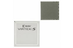
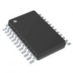
New & Original Virtex-5 Family Overview XC5VSX95T-1FF1136C
|
|
Virtex-5 Family Overview
General Description The Virtex®-5 family provides the newest most powerful features in the FPGA market. Using the second generation ASMBL™ (Advanced Silicon Modular Block) column-based architecture, the Virtex-5 family contains five distinct platforms (sub-families), the most choice offered by any FPGA family. Each platform contains a different ratio of features to address the needs of a wide variety of advanced logic designs. In addition to the most advanced, high-performance logic fabric, Virtex-5 FPGAs contain many hard-IP system level blocks, including powerful 36-Kbit block RAM/FIFOs, second generation 25 x 18 DSP slices, SelectIO™ technology with built-in digitallycontrolled impedance, ChipSync™ source-synchronous interface blocks, system monitor functionality, enhanced clock management tiles with integrated DCM (Digital Clock Managers) and phase-locked-loop (PLL) clock generators, and advanced configuration options. Additional platform dependant features include power-optimized high-speed serial transceiver blocks for enhanced serial connectivity, PCI Express® compliant integrated Endpoint blocks, tri-mode Ethernet MACs (Media Access Controllers), and high-performance PowerPC® 440 microprocessor embedded blocks. These features allow advanced logic designers to build the highest levels of performance and functionality into their FPGA-based systems. Built on a 65-nm state-of-the-art copper process technology, Virtex-5 FPGAs are a programmable alternative to custom ASIC technology. Most advanced system designs require the programmable streCM GROUPh of FPGAs. Virtex-5 FPGAs offer the best solution for addressing the needs of high-performance logic designers, high-performance DSP designers, and high-performance embedded systems designers with unprecedented logic, DSP, hard/soft microprocessor, and connectivity capabilities. The Virtex-5 LXT, SXT, TXT, and FXT platforms include advanced high-speed serial connectivity and link/transaction layer capability
Summary of Virtex-5 FPGA Features • Five platforms LX, LXT, SXT, TXT, and FXT − Virtex-5 LX: High-performance general logic applications − Virtex-5 LXT: High-performance logic with advanced serial connectivity − Virtex-5 SXT: High-performance signal processing applications with advanced serial connectivity − Virtex-5 TXT: High-performance systems with double density advanced serial connectivity − Virtex-5 FXT: High-performance embedded systems with advanced serial connectivity • Cross-platform compatibility − LXT, SXT, and FXT devices are footprint compatible in the same package using adjustable voltage regulators • Most advanced, high-performance, optimal-utilization, FPGA fabric − Real 6-input look-up table (LUT) technology − Dual 5-LUT option − Improved reduced-hop routing − 64-bit distributed RAM option − SRL32/Dual SRL16 option • Powerful clock management tile (CMT) clocking − Digital Clock Manager (DCM) blocks for zero delay buffering, frequency synthesis, and clock phase shifting − PLL blocks for input jitter filtering, zero delay buffering, frequency synthesis, and phase-matched clock division • 36-Kbit block RAM/FIFOs − True dual-port RAM blocks − Enhanced optional programmable FIFO logic − Programmable - True dual-port widths up to x36 - Simple dual-port widths up to x72 − Built-in optional error-correction circuitry − Optionally program each block as two independent 18-Kbit blocks • High-performance parallel SelectIO technology − 1.2 to 3.3V I/O Operation − Source-synchronous interfacing using ChipSync™ technology − Digitally-controlled impedance (DCI) active termination − Flexible fine-grained I/O banking − High-speed memory interface support • Advanced DSP48E slices − 25 x 18, two’s complement, multiplication − Optional adder, subtracter, and accumulator − Optional pipelining − Optional bitwise logical functionality − Dedicated cascade connections • Flexible configuration options − SPI and Parallel FLASH interface − Multi-bitstream support with dedicated fallback reconfiguration logic − Auto bus width detection capability • System Monitoring capability on all devices − On-chip/Off-chip thermal monitoring − On-chip/Off-chip power supply monitoring − JTAG access to all monitored quantities • Integrated Endpoint blocks for PCI Express Designs − LXT, SXT, TXT, and FXT Platforms − Compliant with the PCI Express Base Specification 1.1 − x1, x4, or x8 lane support per block − Works in conjunction with RocketIO™ transceivers • Tri-mode 10/100/1000 Mb/s Ethernet MACs − LXT, SXT, TXT, and FXT Platforms − RocketIO transceivers can be used as PHY or connect to external PHY using many soft MII (Media Independent Interface) options • RocketIO GTP transceivers 100 Mb/s to 3.75 Gb/s − LXT and SXT Platforms • RocketIO GTX transceivers 150 Mb/s to 6.5 Gb/s − TXT and FXT Platforms • PowerPC 440 Microprocessors − FXT Platform only − RISC architecture − 7-stage pipeline − 32-Kbyte instruction and data caches included − Optimized processor interface structure (crossbar) • 65-nm copper CMOS process technology • 1.0V core voltage • High signal-integrity flip-chip packaging available in standard or Pb-free package options
Virtex-5 FPGA Logic • On average, one to two speed grade improvement over Virtex-4 devices • Cascadable 32-bit variable shift registers or 64-bit distributed memory capability • Superior routing architecture with enhanced diagonal routing supports block-to-block connectivity with minimal hops • Up to 330,000 logic cells including: − Up to 207,360 internal fabric flip-flops with clock enable (XC5VLX330) − Up to 207,360 real 6-input look-up tables (LUTs) with greater than 13 million total LUT bits − Two outputs for dual 5-LUT mode gives enhanced utilization − Logic expanding multiplexers and I/O registers
550 MHz Clock Technology • Up to six Clock Management Tiles (CMTs) − Each CMT contains two DCMs and one PLL—up to eighteen total clock generators − Flexible DCM-to-PLL or PLL-to-DCM cascade − Precision clock deskew and phase shift − Flexible frequency synthesis − Multiple operating modes to ease performance trade-off decisions − Improved maximum input/output frequency − Fine-grained phase shifting resolution − Input jitter filtering − Low-power operation − Wide phase shift range • Differential clock tree structure for optimized low-jitter clocking and precise duty cycle • 32 global clock networks • Regional, I/O, and local clocks in addition to global clocks
SelectIO Technology • Up to 1,200 user I/Os • Wide selection of I/O standards from 1.2V to 3.3V • Extremely high-performance − Up to 800 Mb/s HSTL and SSTL (on all single-ended I/Os) − Up to 1.25 Gb/s LVDS (on all differential I/O pairs) • True differential termination on-chip • Same edge capture at input and output I/Os • Extensive memory interface support
550 MHz Integrated Block Memory • Up to 16.4 Mbits of integrated block memory • 36-Kbit blocks with optional dual 18-Kbit mode • True dual-port RAM cells • Independent port width selection (x1 to x72) − Up to x36 total per port for true dual port operation − Up to x72 total per port for simple dual port operation (one Read port and one Write port) − Memory bits plus parity/sideband memory support for x9, x18, x36, and x72 widths − Configurations from 32K x 1 to 512 x 72 (8K x 4 to 512 x 72 for FIFO operation) • Multirate FIFO support logic − Full and Empty flag with fully programmable Almost Full and Almost Empty flags • Synchronous FIFO support without Flag uncertainty • Optional pipeline stages for higher performance • Byte-write capability • Dedicated cascade routing to form 64K x 1 memory without using FPGA routing • Integrated optional ECC for high-reliability memory requirements • Special reduced-power design for 18 Kbit (and below) operation
550 MHz DSP48E Slices • 25 x 18 two’s complement multiplication • Optional pipeline stages for enhanced performance • Optional 48-bit accumulator for multiply accumulate (MACC) operation with optional accumulator cascade to 96-bits • Integrated adder for complex-multiply or multiply-add operation • Optional bitwise logical operation modes • Independent C registers per slice • Fully cascadable in a DSP column without external routing resources
|
| Product Tags: ic programmer circuit programmable audio chip |

