China Flash Memory IC Chip manufacturer
ChongMing Group (HK) Int'l Co., Ltd
CHONGMING GROUP (HK) INT'L CO., LTD.
3
Home > Products > Integrated Circuit Chips >

Integrated Circuit Chip Integrated Synthesizer and VCO ADF4360-4BCPZ

Browse Categories

ChongMing Group (HK) Int'l Co., Ltd

City: shenzhen

Country/Region:china

Tel:86-755-88367702

Contact Person:
Ms.Doris Guo
View Contact Details

Integrated Circuit Chip Integrated Synthesizer and VCO ADF4360-4BCPZ

Model Number ADF4360-4BCPZ
Certification new & original
Place of Origin original factory
Minimum Order Quantity 10pcs
Price Negotiate
Payment Terms T/T, Western Union, Paypal
Supply Ability 3600pcs
Delivery Time 1 day
Packaging Details Please contact me for details
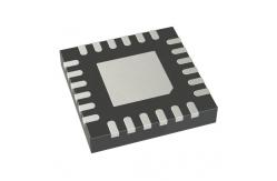
Description Fanout Distribution, Integer N Synthesizer (RF) IC 1.75GHz 1 24-WFQFN Exposed Pad, CSP
Output frequency range 1450 MHz to 1750 MHz
AVDD to GND1 −0.3 V to +3.9 V
AVDD to DVDD −0.3 V to +0.3 V
VVCO to GND −0.3 V to +3.9 V
VVCO to AVDD −0.3 V to +0.3 V
Digital I/O Voltage to GND −0.3 V to VDD + 0.3 V
REFIN to GND −0.3 V to VDD + 0.3 V
Maximum Junction Temperature 150°C
Detailed Product Description


Integrated Synthesizer and VCO ADF4360-4


FEATURES

Output frequency range: 1450 MHz to 1750 MHz

Divide-by-2 output

3.0 V to 3.6 V power supply

1.8 V logic compatibility

Integer-N synthesizer

Programmable dual-modulus prescaler 8/9, 16/17, 32/33

Programmable output power level

3-wire serial interface

Analog and digital lock detect

Hardware and software power-down mode


APPLICATIONS

Wireless handsets (DECT, GSM, PCS, DCS, WCDMA)

Test equipment

Wireless LANs

CATV equipment


GENERAL DESCRIPTION

The ADF4360-4 is a fully integrated integer-N synthesizer and voltage-controlled oscillator (VCO). The ADF4360-4 is designed for a center frequency of 1600 MHz. In addition, a divide-by-2 option is available, whereby the user gets an RF output of between 725 MHz and 875 MHz.


Control of all the on-chip registers is through a simple 3-wire interface. The device operates with a power supply ranging from 3.0 V to 3.6 V and can be powered down when not in use.


FUNCTIONAL BLOCK DIAGRAM


TIMING CHARACTERISTICS 

AVDD = DVDD = VVCO = 3.3 V ± 10%;AGND = DGND = 0 V; 1.8 V and 3 V logic levels used; TA = TMIN to TMAX, unless otherwise noted.

  Parameter Limit at TMIN to TMAX (B Version)    Unit   Test Conditions/Comments

    t1

   20

   ns min   LE Setup Time
    t2   10   ns min   DATA to CLOCK Setup Time
    t3   10   ns min   DATA to CLOCK Hold Time
    t4   25   ns min   CLOCK High Duration
    t5   25   ns min   CLOCK Low Duration
    t6   10   ns min   CLOCK to LE Setup Time
    t7   20   ns min   LE Pulse Width


ABSOLUTE MAXIMUM RATINGS TA = 25°C, unless otherwise noted.

               Parameter                                                                 Rating

     AVDD to GND1                                                                −0.3 V to +3.9 V

     AVDD to DVDD                                                                −0.3 V to +0.3 V

     VVCO to GND                                                                 −0.3 V to +3.9 V

     VVCO to AVDD                                                                −0.3 V to +0.3 V

     Digital I/O Voltage to GND                                    −0.3 V to VDD + 0.3 V

    Analog I/O Voltage to GND                                    −0.3 V to VDD + 0.3 V

    REFIN to GND                                                       −0.3 V to VDD + 0.3 V

    Operating Temperature Range

          Maximum Junction Temperature                                   150°C

    CSP θJA Thermal Impedance

         (Paddle Soldered)                                                           50°C/W

         (Paddle Not Soldered)                                                     88°C/W

    Lead Temperature, Soldering

          Vapor Phase (60 sec)                                                     215°C

          Infrared (15 sec)                                                              220°C

1 GND = AGND = DGND = 0 V.


Stresses above those listed under Absolute Maximum Ratings may cause permanent damage to the device. This is a stress rating only; functional operation of the device at these or any other conditions above those indicated in the operational sections of this specification is not implied. Exposure to absolute maximum rating conditions for extended periods may affect device reliability. This device is a high performance RF integrated circuit with an ESD rating of <1 kV and it is ESD sensitive. Proper precautions should be taken for handling and assembly.


Product Tags: circuit board ic   electronic chip board  
Related Products
Email to this supplier
 
From:
Enter your Email please.
To: ChongMing Group (HK) Int'l Co., Ltd
Subject:
Message:
Characters Remaining: (80/3000)