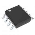
74AUP1G157GW,125 Circuit Board Chips Low power 2-input multiplexer IC Chip
|
|
74AUP1G157 Low-power 2-input multiplexer
1. General description
The 74AUP1G157 is a high-performance, low-power, low-voltage, Si-gate CMOS device, superior to most advanced CMOS compatible TTL families. Schmitt trigger action at all inputs makes the circuit tolerant to slower input rise and fall times across the entire VCC range from 0.8 V to 3.6 V.
This device ensures a very low static and dynamic power consumption across the entire VCC range from 0.8 V to 3.6 V. This device is fully specified for partial power-down applications using IOFF.
The IOFF circuitry disables the output, preventing the damaging backflow current through the device when it is powered down.
The 74AUP1G157 is a single 2-input multiplexer which select data from two data inputs (I0 and I1) under control of a common data select input (S).
The state of the common data select input determines the particular register from which the data comes. The output (Y) presents the selected data in the true (non-inverted) form.
2. Features
■ Wide supply voltage range from 0.8 V to 3.6 V ■ High noise immunity ■ Complies with JEDEC standards: ◆ JESD8-12 (0.8 V to 1.3 V) ◆ JESD8-11 (0.9 V to 1.65 V) ◆ JESD8-7 (1.2 V to 1.95 V) ◆ JESD8-5 (1.8 V to 2.7 V) ◆ JESD8-B (2.7 V to 3.6 V)
■ ESD protection: ◆ HBM JESD22-A114-D Class 3A exceeds 4000 V ◆ MM JESD22-A115-A exceeds 200 V ◆ CDM JESD22-C101-C exceeds 1000 V
■ Low static power consumption; ICC = 0.9 µA (maximum) ■ Latch-up performance exceeds 100 mA per JESD 78 Class II ■ Inputs accept voltages up to 3.6 V ■ Low noise overshoot and undershoot < 10 % of VCC ■ IOFF circuitry provides partial Power-down mode operation ■ Multiple package options ■ Specified from −40 °C to +85 °C and −40 °C to +125 °C
A part of stock list
|
||||||||||||||||||||||||||||||||||||||||||||||||||||||||||||||||||||||||||||||||||||||||||||||||||||||||||||||||||||||||
| Product Tags: electronic chip board electronic components ic |