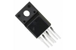
Green Mode Fairchild Power Switch Field Effect Transistor ,
FSDM0465R
Features
- Internal Avalanche Rugged SenseFET
- Low Start-up Current (max. 40µA)
- Low Power Consumption; under 1W at 240VAC and 0.4W Load
- Precise Fixed Operating
- Frequency (66kHz) Frequency Modulation for Low EMI
- Pulse-by-Pulse Current Limiting (Adjustable)
- Over-Voltage Protection (OVP)
- Overload Protection (OLP)
- Thermal Shutdown Function (TSD)
- Auto-Restart Mode
- Under-Voltage Lock Out (UVLO) with Hysteresis
- Built-in Soft-Start (15ms)
Applications
- SMPS for VCR, SVR, STB, DVD, and DVCD
- Adaptor
- SMPS for LCD Monitor
Related Application Notes
- AN-4137: Design Guidelines for Off-line Flyback Converters Using
Fairchild Power Switch (FPS)
- AN-4140: Transformer Design Consideration for Off-line Flyback
Converters using Fairchild Power Switch
- AN-4141: Troubleshooting and Design Tips for Fairchild Power
Switch Flyback Applications
- AN-4148: Audible Noise Reduction Techniques for FPS Applications
Description
The FSCM0465R is an integrated Pulse-Width Modulator (PWM) and
SenseFET specifically designed for high-performance offline Switch
Mode Power Supplies (SMPS) with minimal external components. This
device is an integrated high-voltage powerswitching regulator that
combines an avalanche rugged SenseFET with a current mode PWM
control block. The PWM controller includes an integrated
fixed-frequency oscillator, under-voltage lockout, leading edge
blanking (LEB), optimized gate driver, internal soft-start,
temperature-compensated precise current sources for a loop
compensation, and self-protection circuitry. Compared with a
discrete MOSFET and PWM controller solution, it can reduce total
cost, component count, size, and weight while simultaneously
increasing efficiency, productivity, and system reliability. This
device is a basic platform well suited for cost-effective designs
of flyback converters.
Absolute Maximum Ratings
The “Absolute Maximum Ratings” are those values beyond which the
safety of the device cannot be guaranteed. The device should not be
operated at these limits. The parametric values defined in the
Electrical Characteristics tables are not guaranteed at the
absolute maximum ratings.
TA = 25°C unless otherwise specified.
| Symbol | Parameter | Value | Unit |
| BVDSS | Drain-Source Breakdown Voltage(1) | 650 | V |
| VDGR | Drain-Gate Voltage (RGS=1MΩ) | 650 | V |
| VGS | Gate-Source (GND) Voltage | ±30 | V |
| IDM | Drain Current Pulsed(2) | 16 | ADC |
| ID | Continuous Drain Current
(TO-220-6L, I2-PAK-6L) | T C = 25°C | 4.0 | ADC |
| T C = 100°C | 2.5 | ADC |
| Continuous Drain Current (D2-PAK-6L) | T C = 25°C | 2.3 | ADC |
| T C = 100°C | 1.4 | ADC |
| VCC | Supply Voltage | 20 | V |
| VFB | Feedback Voltage Range | -0.3 to VCC | V |
| PD | Total Power Dissipation (TO-220-6L) | 140 | W |
| Derating | -1.1 | W/°C |
| PD | Total Power Dissipation (I2-PAK-6L) | 75 | W |
| Derating | -1.5 | W/°C |
| PD | Total Power Dissipation (D2-PAK-6L) | 80 | W |
| Derating | -0.64 | W/°C |
| TJ | Operating Junction Temperature | Internally limited | °C |
| TA | Operating Ambient Temperature | -25 to +85 | °C |
| TSTG | Storage Temperature | -55 to +150 | °C |
| | ESD Capability, HBM Model (All pins except Vfb) | 2.0 (GND-Vfb = 1.5kV) (VCC-Vfb = 1.0kV) | kV |
| | ESD Capability, Machine Model (All pins except Vfb) | 300 (GND-Vfb = 250V) (VCC-Vfb = 100V) | V |
Notes: 1. Tj = 25°C to 150°C
2. Repetitive
rating: Pulse-width limited by maximum junction temperature
3. T C: Case back surface temperature with infinite heat sink
Typical Circuit
Figure 1. Typical Flyback Application
Internal Block Diagram
Figure 2. Functional Block Diagram of FSCM0465R
Pin Configuration
Figure 3. Pin Configuration (Top View)