
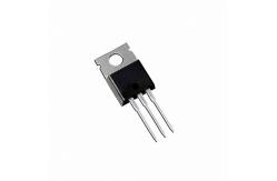
Trench Power Mosfet IC IRF1404PBF Advanced Ultra Low On-Resistance
|
|
Trench Power Mosfet IC IRF1404PBF Advanced Ultra Low On-Resistance
Description Seventh Generation HEXFETÆ Power MOSFETs from International Rectifier utilize advanced processing techniques to achieve extremely low on-resistance per silicon area. This benefit, combined with the fast switching speed and ruggedized device design that HEXFET power MOSFETs are well known for, provides the designer with an extremely efficient and reliable device for use in a wide variety of applications including automotive.
The TO-220 package is universally preferred for all automotive-commercial-industrial applications at power dissipation levels to approximately 50 watts. The low thermal resistance and low package cost of the TO-220 contribute to its wide acceptance throughout the industry.
Advanced Process Technology Ultra Low On-Resistance Dynamic dv/dt Rating 175°C Operating Temperature Fast Switching Fully Avalanche Rated Automotive Qualified (Q101) Lead-Free
Notes on Repetitive Avalanche Curves , Figures 15, 16: (For further info, see AN-1005 at www.irf.com)
1. Avalanche failures assumption: Purely a thermal phenomenon and failure occurs at a temperature far in excess of Tjmax. This is validated for every part type.
2. Safe operation in Avalanche is allowed as long asTjmax is not exceeded.
3. Equation below based on circuit and waveforms shown in Figures 12a, 12b.
4. PD (ave) = Average power dissipation per single avalanche pulse.
5. BV = Rated breakdown voltage (1.3 factor accounts for voltage increase during avalanche).
6. Iav = Allowable avalanche current.
7. ∆T = Allowable rise in junction temperature, not to exceed Tjmax (assumed as 25°C in Figure 15, 16). tav = Average time in avalanche. D = Duty cycle in avalanche = tav ·f ZthJC(D, tav) = Transient thermal resistance, see figure 11)
|
||||||||||||||||||
| Product Tags: npn smd transistor silicon power transistors |
|
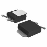
RB450FT106 Rectifier Diode Schottky barrier diode diode laser hair removal |
|
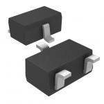
TK10P60W Power Mosfet Transistor MOSFETs Silicon N-Channel MOS |
|
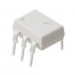
4N25M Electronic IC Chips General Purpose Phototransistor Optocouplers |
|
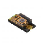
TEMT6000X01 Electronic IC Chips Ambient Light Sensor, RoHS Compliant |
|
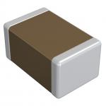
GRM033R71C272KA88D NEW AND ORIGINAL STOCK |
|
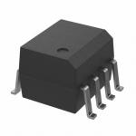
FOD2742B Flash Memory IC NEW AND ORIGINAL STOCK |